SCHS240D November   1998  – October 2024 CD54AC164 , CD54ACT164 , CD74AC164 , CD74ACT164

PRODUCTION DATA  

  1.   1
  2. Features
  3. Description
  4. Pin Configuration and Functions
  5. Specifications
    1. 4.1 Absolute Maximum Ratings
    2. 4.2 ESD Ratings
    3. 4.3 Recommended Operating Conditions
    4. 4.4 Thermal Information
    5. 4.5 DC Electrical Specifications
    6. 4.6 Prerequisite for Switching Function
    7. 4.7 Switching Specifications
  6. Parameter Measurement Information
  7. Detailed Description
    1. 6.1 Overview
    2. 6.2 Functional Block Diagram
    3. 6.3 Feature Description
      1. 6.3.1 Standard CMOS Inputs
      2. 6.3.2 TTL-Compatible CMOS Inputs
    4. 6.4 Device Functional Modes
  8. Application and Implementation
    1. 7.1 Application Information
    2. 7.2 Typical Application
      1. 7.2.1 Design Requirements
        1. 7.2.1.1 Power Considerations
        2. 7.2.1.2 Input Considerations
        3. 7.2.1.3 Output Considerations
        4. 7.2.1.4 Application Curve
    3. 7.3 Power Supply Recommendations
    4. 7.4 Layout
      1. 7.4.1 Layout Guidelines
      2. 7.4.2 Layout Example
  9. Device and Documentation Support
    1. 8.1 Documentation Support
      1. 8.1.1 Related Documentation
    2. 8.2 Receiving Notification of Documentation Updates
    3. 8.3 Support Resources
    4. 8.4 Trademarks
    5. 8.5 Electrostatic Discharge Caution
    6. 8.6 Glossary
  10. Device and Documentation Support
    1. 9.1 Documentation Support (Analog)
      1. 9.1.1 Related Documentation
    2. 9.2 Receiving Notification of Documentation Updates
    3. 9.3 Support Resources
    4. 9.4 Trademarks
    5. 9.5 Electrostatic Discharge Caution
    6. 9.6 Glossary
  11. 10Revision History
  12. 11Mechanical, Packaging, and Orderable Information

Refer to the PDF data sheet for device specific package drawings

Mechanical Data (Package|Pins)
  • D|14
  • PW|14
  • BQA|14
  • N|14
Thermal pad, mechanical data (Package|Pins)

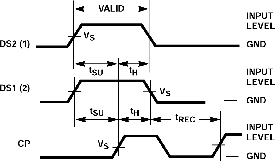
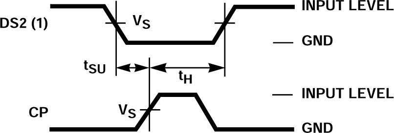
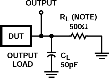
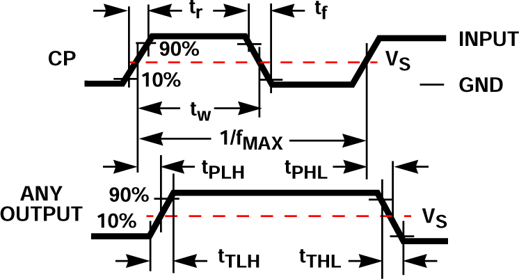
Parameter Measurement Information

Load Circuit And Voltage Waveforms
CD54AC164 CD74AC164 CD54ACT164 CD74ACT164 CD54AC164 CD74AC164 CD54ACT164 CD74ACT164

CD54AC164 CD74AC164 CD54ACT164 CD74ACT164 Propagation Delay
                        Times

For AC Series Only: When VCC = 1.5V, RL = 1kΩ.For AC Series Only: When VCC = 1.5V, RL = 1kΩ.For AC Series Only: When VCC = 1.5V, RL = 1kΩ.

Figure 5-1 Propagation Delay Times
Table 5-1 Propagation Delay Times
AC ACT
Input Level VCC 3V
Input Switching Voltage, VS 0.5 VCC 1.5V
Output Switching Voltage, VS 0.5 VCC 0.5 VCC