SCHS246A August 1998 – August 2024 CD74AC251
PRODUCTION DATA
- 1
- 1 Features
- 2 Description
- 3 Pin Configuration and Functions
- 4 Specifications
- 5 Parameter Measurement Information
- 6 Detailed Description
- 7 Application and Implementation
- 8 Device and Documentation Support
- 9 Revision History
- 10Mechanical, Packaging, and Orderable Information
Refer to the PDF data sheet for device specific package drawings
Mechanical Data (Package|Pins)
- D|16
Thermal pad, mechanical data (Package|Pins)
2 Description
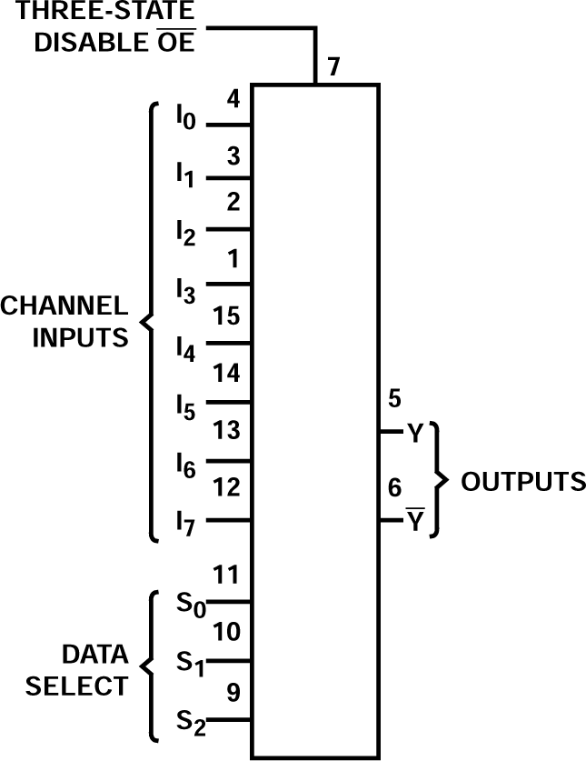
The CD74AC251 8-input multiplexers that utilize the Harris Advanced CMOS Logic technology. This multiplexer features both true (Y) and complement (Y) outputs as well as an Output Enable (OE) input. The OE must be at a LOW logic level to enable this device. When the OE input is HIGH, both outputs are in the high-impedance state. When enabled, address information on the data select inputs determines which data input is routed to the Y and Y outputs.
Package Information
| PART NUMBER | PACKAGE(1) | PACKAGE SIZE(2) | BODY SIZE(3) |
|---|---|---|---|
| CD74AC251 | D (SOIC, 16) | 9.9mm × 6mm | 9.9mm × 3.9mm |
(1) For more information, see Section 10.
(2) The package size (length × width) is a nominal value and
includes pins, where applicable.
(3) The body size (length × width) is
a nominal value and does not include pins.
 Functional Diagram