SCHS338A March 2003 – August 2024 CD54ACT151 , CD74ACT151
PRODUCTION DATA
- 1
- 1 Features
- 2 Description
- 3 Pin Configuration and Functions
- 4 Specifications
- 5 Parameter Measurement Information
- 6 Detailed Description
- 7 Application and Implementation
- 8 Device and Documentation Support
- 9 Revision History
- 10Mechanical, Packaging, and Orderable Information
Package Options
Refer to the PDF data sheet for device specific package drawings
Mechanical Data (Package|Pins)
- D|16
Thermal pad, mechanical data (Package|Pins)
Orderable Information
2 Description
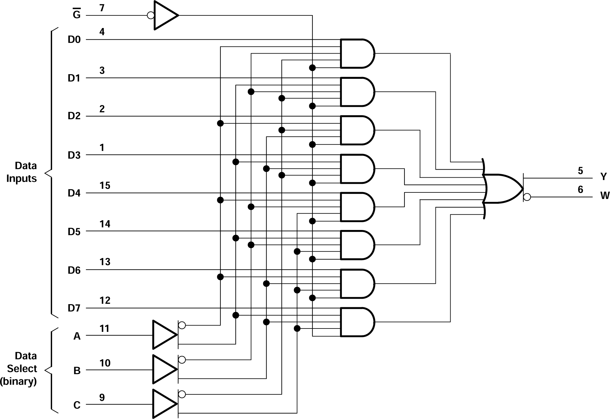
These data selectors/multiplexers provide full binary decoding to select one of eight data sources. The strobe (G) input must be at a low logic level to enable the inputs. A high level at the strobe terminal forces the W output high and the Y output low.
Device
Information
| PART NUMBER | PACKAGE(1) | PACKAGE SIZE(2) | BODY SIZE(3) |
|---|---|---|---|
| CDx4ACT151 | D (SOIC, 16) | 8.65mm × 6mm | 8.65mm × 3.9mm |
| J (CDIP , 16) | 19.55mm x 7.9mm | 19.55 mm x 6.7mm |
(1) For more information, see Mechanical, Packaging, and Orderable Information.
(2) The package size (length × width) is a
nominal value and includes pins, where applicable.
(3) The body size (length × width) is a
nominal value and does not include pins.
 Logic
Diagram (Positive Logic)