SCHS345A April 2003 – May 2024 CD74ACT175
PRODUCTION DATA
- 1
- 1 Features
- 2 Applications
- 3 Description
- 4 Pin Configurations and Functions
- 5 Specifications
- 6 Parameter Measurement Information
- 7 Detailed Description
- 8 Application and Implementation
- 9 Device and Documentation Support
- 10Revision History
- 11Mechanical, Packaging, and Orderable Information
Package Options
Refer to the PDF data sheet for device specific package drawings
Mechanical Data (Package|Pins)
- N|16
- D|16
Thermal pad, mechanical data (Package|Pins)
Orderable Information
3 Description
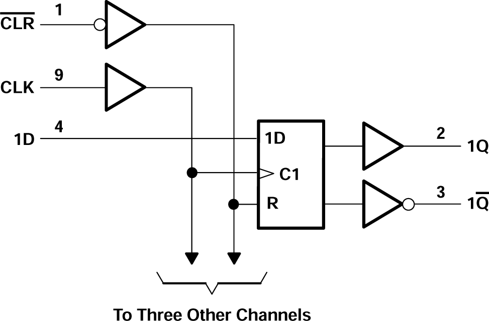
This positive-edge-triggered D-type flip-flop has a direct clear (CLR) input. The CD74ACT175 features complementary outputs from each flip-flop.
Package Information
| PART NUMBER | PACKAGE(1) | PACKAGE SIZE(2) | BODY SIZE(3) |
|---|---|---|---|
| CD74ACT175 | N (PDIP, 16) | 19.3mm × 9.4mm | 19.3mm × 6.35mm |
| D (SOIC, 16) | 9.9mm × 6mm | 9.9mm × 3.9mm |
(1) For more information, see Section
11.
(2) The package size (length × width)
is a nominal value and includes pins, where applicable.
(3) The body size (length × width) is a nominal value and does not include pins.
 Logic Diagram (Positive
Logic)