SCHS345A April 2003 – May 2024 CD74ACT175
PRODUCTION DATA
- 1
- 1 Features
- 2 Applications
- 3 Description
- 4 Pin Configurations and Functions
- 5 Specifications
- 6 Parameter Measurement Information
- 7 Detailed Description
- 8 Application and Implementation
- 9 Device and Documentation Support
- 10Revision History
- 11Mechanical, Packaging, and Orderable Information
Package Options
Refer to the PDF data sheet for device specific package drawings
Mechanical Data (Package|Pins)
- N|16
- D|16
Thermal pad, mechanical data (Package|Pins)
Orderable Information
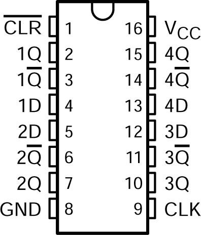
4 Pin Configurations and Functions
 Figure 4-1 D or N Package, 16-PIN
SCOIC or PDIP (Top View)
Figure 4-1 D or N Package, 16-PIN
SCOIC or PDIP (Top View)Table 4-1 Pin Functions
| PIN | TYPE | DESCRIPTION | |
|---|---|---|---|
| NO. | NAME | ||
| 1 | CLR | I | Clear Pin |
| 2 | 1Q | O | 1Q Output |
| 3 | 1Q | O | 1Q Output |
| 4 | 1D | I | 1D Input |
| 5 | 2D | I | 2D Input |
| 6 | 2Q | O | 2Q Output |
| 7 | 2Q | O | 2Q Output |
| 8 | GND | — | Ground Pin |
| 9 | CLK | I | Clock Input |
| 10 | 3Q | O | 3Q Output |
| 11 | 3Q | O | 3QOutput |
| 12 | 3D | I | 3D Input |
| 13 | 4D | I | 4D Input |
| 14 | 4Q | O | 4QOutput |
| 15 | 4Q | O | 4Q Output |
| 16 | VCC | — | Power Pin |