SCHS245D November 1998 – April 2024 CD54AC245 , CD54ACT245 , CD74AC245 , CD74ACT245
PRODMIX
- 1
- 1 Features
- 2 Description
- 3 Pin Configuration and Functions
- 4 Specifications
- 5 Parameter Measurement Information
- 6 Detailed Description
- 7 Application and Implementation
- 8 Device and Documentation Support
- 9 Revision History
- 10Mechanical, Packaging, and Orderable Information
Refer to the PDF data sheet for device specific package drawings
Mechanical Data (Package|Pins)
- DB|20
- N|20
- DW|20
Thermal pad, mechanical data (Package|Pins)
2 Description
The 'AC245 and 'ACT245 are octal-bus transceivers that utilize Advanced CMOS Logic technology.
Device Information
| PART NUMBER | PACKAGE(1) | PACKAGE SIZE(2) | BODY SIZE(3) |
|---|---|---|---|
| CD74AC245/ CD74ACT245 | N (PDIP, 20) | 24.33mm × 9.4mm | 24.33mm × 6.35mm |
| DW (SOIC, 20) | 12.80mm × 10.3mm | 12.80mm × 7.50mm | |
| CD54AC245/ CD54ACT245 | J (CDIP, 20) | 24.2mm × 7.62mm | 24.2mm × 6.92mm |
| CD74ACT245 | DB (SSOP, 20) | 7.2mm × 7.8mm | 7.2mm × 5.3mm |
(1) For more information, see Section 11.
(2) The package size (length × width)
is a nominal value and includes pins, where applicable.
(3) The body size (length × width) is
a nominal value and does not include pins.
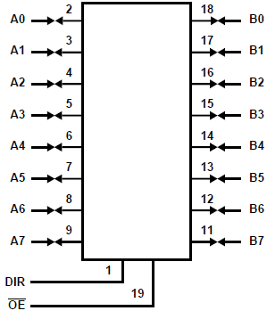
 Logic Diagram (Positive
Logic)