SCHS245D November 1998 – April 2024 CD54AC245 , CD54ACT245 , CD74AC245 , CD74ACT245
PRODMIX
- 1
- 1 Features
- 2 Description
- 3 Pin Configuration and Functions
- 4 Specifications
- 5 Parameter Measurement Information
- 6 Detailed Description
- 7 Application and Implementation
- 8 Device and Documentation Support
- 9 Revision History
- 10Mechanical, Packaging, and Orderable Information
Refer to the PDF data sheet for device specific package drawings
Mechanical Data (Package|Pins)
- DB|20
- N|20
- DW|20
Thermal pad, mechanical data (Package|Pins)
4.6 Timing Diagrams

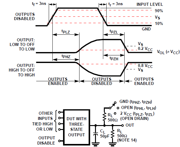
 Figure 4-1 THREE-STATE PROPAGATION DELAY TIMES AND TEST CIRCUIT
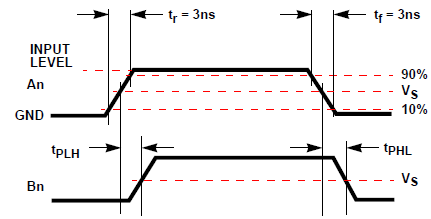
 Figure 4-3 PROPAGATION DELAY TIMES
Table 4-1
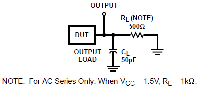
Figure 4-4 PROPAGATION DELAY TIMES| AC | ACT | |
|---|---|---|
| Input Level | VCC | 3V |
| Input Switching Voltage, VS | 0.5 VCC | 1.5V |
| Output Switching Voltage, VS | 0.5 VCC | 0.5 VCC |