SCHS248B November 1998 – August 2024 CD54AC257 , CD54ACT257 , CD74AC257 , CD74ACT257 , CD74ACT258
PRODUCTION DATA
- 1
- 1 Features
- 2 Description
- 3 Pin Configuration and Functions
- 4 Specifications
- 5 Parameter Measurement Information
- 6 Detailed Description
- 7 Application and Implementation
- 8 Device and Documentation Support
- 9 Revision History
- 10Mechanical, Packaging, and Orderable Information
Package Options
Refer to the PDF data sheet for device specific package drawings
Mechanical Data (Package|Pins)
- N|16
- D|16
Thermal pad, mechanical data (Package|Pins)
Orderable Information
5 Parameter Measurement Information
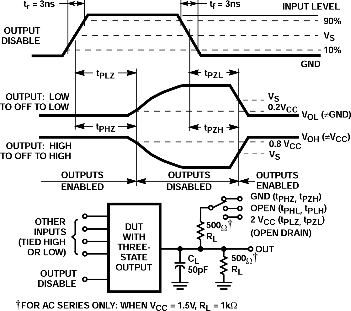
 Figure 5-1 Three-State Propagation Delay Times and Test Circuit
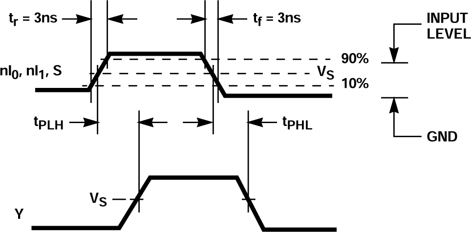
 Figure 5-2 inputs or select to output propagation delays (ac/act257)
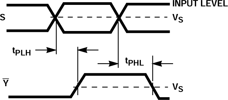
 Figure 5-3 Select to Output Propagation Delays (CD74ACT258)
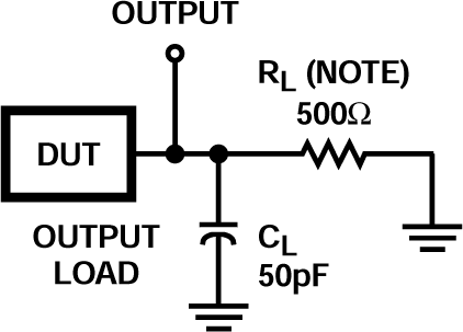
 Figure 5-4
 For AC Series Only: When VCC = 1.5V, RL = 1kW.
| TEST | S1 |
|---|---|
| tPLH/tPHL | Open |
| tPLZ/tPZL | 2 × VCC |
| tPHZ/tPZH | GND |