SCHS285B December 1998 – May 2024 CD54AC541 , CD54ACT540 , CD54ACT541 , CD74AC540 , CD74AC541 , CD74ACT540 , CD74ACT541
PRODUCTION DATA
- 1
- 1 Features
- 2 Description
- 3 Pin Configuration and Functions
- 4 Specifications
- 5 Parameter Measurement Information
- 6 Detailed Description
- 7 Application and Implementation
- 8 Device and Documentation Support
- 9 Revision History
- 10Mechanical, Packaging, and Orderable Information
Package Options
Mechanical Data (Package|Pins)
Thermal pad, mechanical data (Package|Pins)
Orderable Information
2 Description
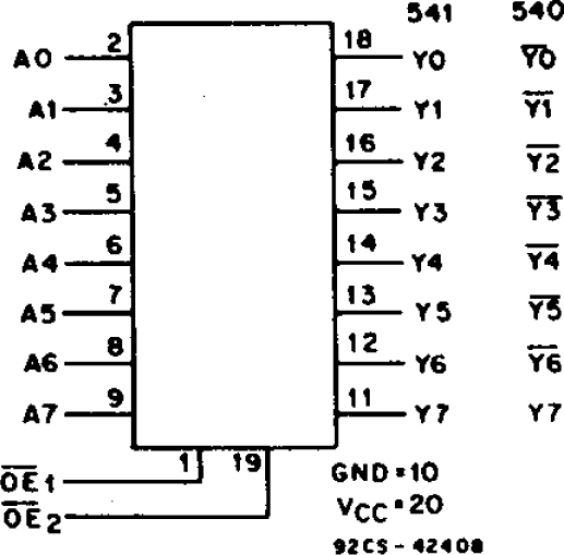
The CD54/74AC540, -541, and CD54/74ACT540, -541 octal buffer/line drivers use the RCA ADVANCED CMOS technology. The CD54/74AC/ACT540 are inverting 3-state buffers having two active-LOW output enables. The CD54/74AC/ACT541 are non-inverting 3-state buffers having two active-LOW output enables.
Device Information
| PART NUMBER | PACKAGE(1) | PACKAGE SIZE(2) | BODY SIZE(3) |
|---|---|---|---|
| CD74AC540, CDx4ACT54x, CDx4AC541 | DW (SOIC, 20) | 12.8mm x 10.3mm | 12.8mm x 7.5mm |
| DB (SSOP, 20) | 7.2mm x 7.8mm | 7.2mm x 5.3mm | |
| N (PDIP, 20) | 24.33mm x 9.4mm | 24.33mm x 6.35mm |
(1) For all available packages, see
Section 10.
(2) The package size (length × width)
is a nominal value and includes pins, where applicable.
(3) The body size (length × width) is
a nominal value and does not include pins.
 Functional Block Diagram