SCHS382A January 2010 – August 2022 CD74HC366-Q1
PRODUCTION DATA
- 1 Features
- 2 Description
- 3 Revision History
- 4 Pin Configuration and Functions
- 5 Specifications
- 6 Parameter Measurement Information
- 7 Detailed Description
- 8 Power Supply Recommendations
- 9 Layout
- 10Device and Documentation Support
- 11Mechanical, Packaging, and Orderable Information
Package Options
Mechanical Data (Package|Pins)
- D|16
Thermal pad, mechanical data (Package|Pins)
Orderable Information
2 Description
The CD74HC365-Q1, CD74HC366-Q1, and CD74HCT365-Q1 silicon gate CMOS three state buffers are general purpose high-speed non-inverting and inverting buffers. They have high drive current outputs which enable high speed operation even when driving large bus capacitances. These circuits possess the low power dissipation of CMOS circuitry, yet have speeds comparable to low power Schottky TTL circuits. Both circuits are capable of driving up to 15 low power Schottky inputs.
Device Information
| PART NUMBER | PACKAGE(1) | BODY SIZE (NOM) |
|---|---|---|
| CD74HC366QDRQ1 | D (SOIC, 16) | 9.90 mm × 3.90 mm |
(1) For all available packages, see the orderable addendum at the
end of the data sheet.
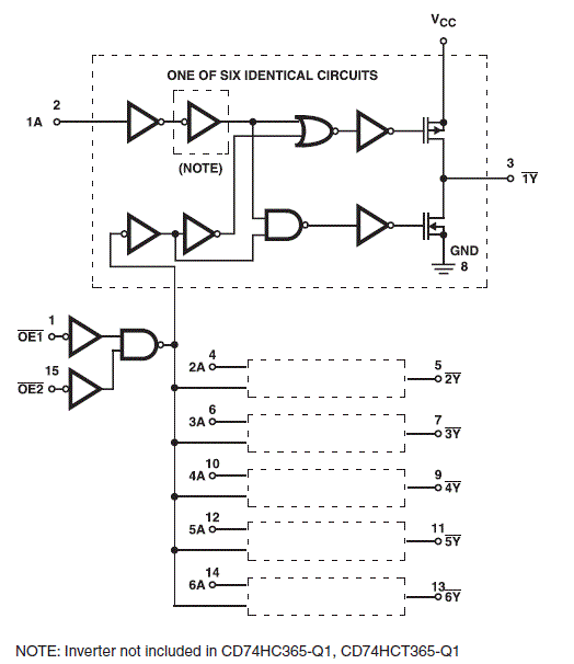
 Functional Block
Diagram