SCHS185E September 1997 – April 2022 CD54HCT390 , CD74HC390 , CD74HCT390
PRODUCTION DATA
- 1 Features
- 2 Description
- 3 Revision History
- 4 Pin Configuration and Functions
- 5 Specifications
- 6 Parameter Measurement Information
- 7 Detailed Description
- 8 Power Supply Recommendations
- 9 Layout
- 10Device and Documentation Support
- 11Mechanical, Packaging, and Orderable Information
Package Options
Refer to the PDF data sheet for device specific package drawings
Mechanical Data (Package|Pins)
- N|16
- D|16
Thermal pad, mechanical data (Package|Pins)
Orderable Information
2 Description
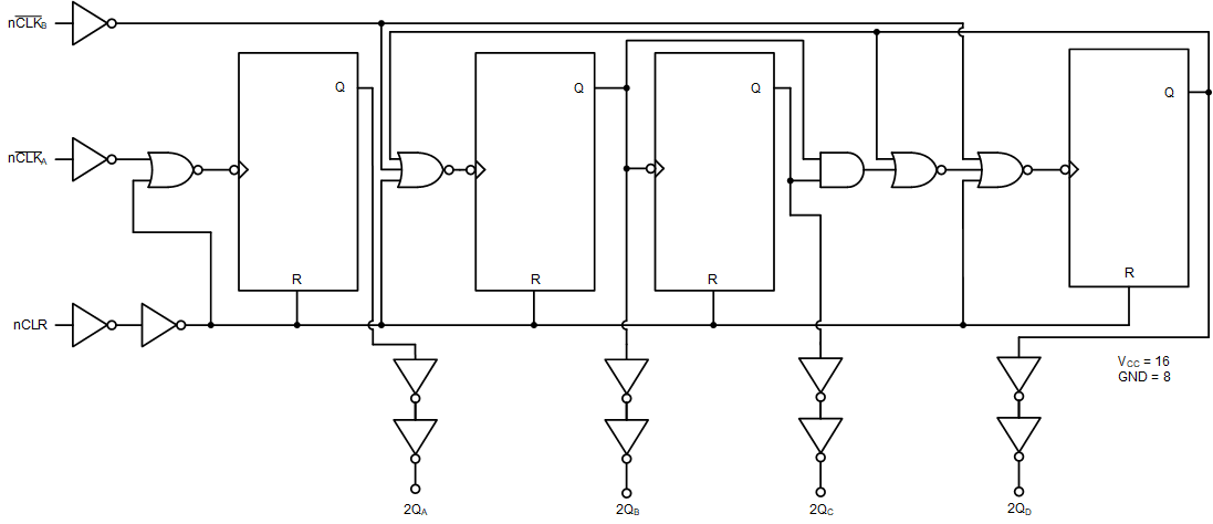
The SN74HC390 and ‘HCT390 devices include two independent 4-bit decade ripple counters, falling-edge clocked with asynchronous clear. Each counter is divided into two sections, a divide-by-2 and divide-by-5 counter, each of which has an independent clock input. This allows for very flexible configuration of the device.
Device Information
| PART NUMBER | PACKAGE(1) | BODY SIZE (NOM) |
|---|---|---|
| CD54HCT390F3A | CDIP (16) | 24.38 mm × 6.92 mm |
| CD74HC390M | SOIC (16) | 9.90 mm × 3.90 mm |
| CD74HCT390M | SOIC (16) | 9.90 mm × 3.90 mm |
| CD74HC390E | PDIP (16) | 19.31 mm × 6.35 mm |
| CD74HCT390E | PDIP (16) | 19.31 mm × 6.35 mm |
(1) For all
available packages, see the orderable addendum at the end of the data
sheet.
 Functional Block
Diagram