SCHS203E November 1998 – July 2022 CD54HC4040 , CD54HCT4040 , CD74HC4040 , CD74HCT4040
PRODUCTION DATA
- 1 Features
- 2 Description
- 3 Revision History
- 4 Pin Configuration and Functions
- 5 Specifications
- 6 Parameter Measurement Information
- 7 Detailed Description
- 8 Power Supply Recommendations
- 9 Layout
- 10Device and Documentation Support
- 11Mechanical, Packaging, and Orderable Information
Package Options
Refer to the PDF data sheet for device specific package drawings
Mechanical Data (Package|Pins)
- N|16
- D|16
Thermal pad, mechanical data (Package|Pins)
Orderable Information
2 Description
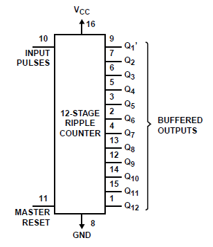
The ’HC4040 and ’HCT4040 are 14-stage ripple-carry binary counters. All counter stages are controller flipflops. The state of the stage advances one count on the negative clock transition of each input pulse; a high voltage level on the MR line resets all counters to their zero state. All inputs and outputs are buffered.
Device Information
| PART NUMBER | PACKAGE(1) | BODY SIZE (NOM) |
|---|---|---|
| CD54HC4040 | J (CDIP, 16) | 24.38 mm × 6.92 mm |
| CD54HCT4040 | J (CDIP, 16) | 24.38 mm × 6.92 mm |
| CD74HC4040 | D (SOIC, 16) | 9.90 mm × 3.90 mm |
| N (PDIP, 16) | 19.31 mm × 6.35 mm | |
| CD74HCT4040 | D (SOIC, 16) | 9.90 mm × 3.90 mm |
| N (PDIP, 16) | 19.31 mm × 6.35 mm |
(1) For all
available packages, see the orderable addendum at the end of the data
sheet.
 Functional Block
Diagram