SCHS208E February 1998 – July 2024 CD54HC4066 , CD74HC4066 , CD74HCT4066
PRODUCTION DATA
- 1
- 1 Features
- 2 Applications
- 3 Description
- 4 Pin Configuration and Functions
- 5 Absolute Maximum Ratings
- 6 ESD Ratings
- 7 Thermal Information
- 8 Recommended Operating Conditions
- 9 Electrical Characteristics: HC Devices
- 10Electrical Characteristics: HCT Devices
- 11Switching Characteristics HC
- 12Switching Characteristics HCT
- 13Analog Channel Specifications
- 14Analog Test Circuits
- 15Test Circuits and Waveforms
- 16Detailed Description
- 17Device and Documentation Support
- 18Revision History
- 19Mechanical, Packaging, and Orderable Information
Package Options
Mechanical Data (Package|Pins)
Thermal pad, mechanical data (Package|Pins)
Orderable Information
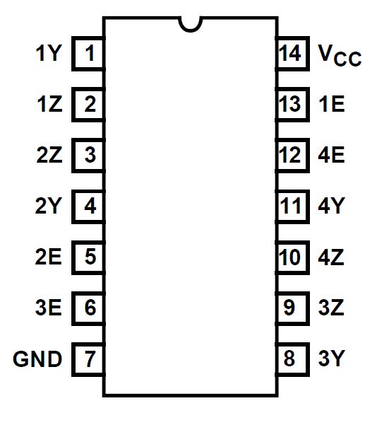
4 Pin Configuration and Functions
 Figure 4-1 CD74HC4066 D or PW Package,
14-Pin SOIC or TSSOP CD74HCT4066 r D Package, 14-Pin SOIC (Top View)
Figure 4-1 CD74HC4066 D or PW Package,
14-Pin SOIC or TSSOP CD74HCT4066 r D Package, 14-Pin SOIC (Top View)Table 4-1 Pin Functions
| PIN | TYPE(1) | DESCRIPTION | |
|---|---|---|---|
| NAME | NO. | ||
| 1Y | 1 | I/O | Input/Output for Switch 1 |
| 1Z | 2 | I/O | Input/Output for Switch 1 |
| 2Z | 3 | I/O | Input/Output for Switch 2 |
| 2Y | 4 | I/O | Input/Output for Switch 2 |
| 2E | 5 | I | Control pin for Switch 2 |
| 3E | 6 | I | Control pin for Switch 3 |
| GND | 7 | - |
Ground Pin |
| 3Y | 8 | I/O | Input/Output for Switch 3 |
| 3Z | 9 | I/O | Input/Output for Switch 3 |
| 4Z | 10 | I/O | Input/Output for Switch 4 |
| 4Y | 11 | I/O | Input/Output for Switch 4 |
| 4E | 12 | I | Control pin for Switch 4 |
| 1E | 13 | I | Control pin for Switch 1 |
| VCC | 14 | - | Power Pin |
(1) Signal Types: I = Input, O = Output, I/O = Input or
Output.