SCHS212E February 1998 – July 2024 CD54HC4316 , CD74HC4316 , CD74HCT4316
PRODUCTION DATA
- 1
- 1 Features
- 2 Description
- 3 Pin Configurations and Functions
- 4 Absolute Maximum Ratings
- 5 Thermal Information
- 6 Recommended Operating Conditions
- 7 Electrical Characteristics: HC Devices
- 8 Electrical Characteristics: HCT Devices
- 9 Switching Characteristics HC
- 10Switching Characteristics HCT
- 11Analog Channel Specifications
- 12HCT Input Loading Table
- 13Recommended Operating Area as a Function of Supply Voltage
- 14Typical Performance Curves
- 15Parameter Measurement Information
- 16Detailed Description
- 17Device and Documentation Support
- 18Revision History
- 19Mechanical, Packaging, and Orderable Information
Package Options
Refer to the PDF data sheet for device specific package drawings
Mechanical Data (Package|Pins)
- PW|16
- NS|16
- N|16
- D|16
Thermal pad, mechanical data (Package|Pins)
Orderable Information
15 Parameter Measurement Information
 Figure 15-1 Crosstalk Between Two Switches
Test Circuit
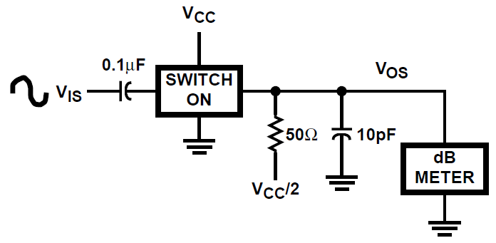 Figure 15-2 Frequency Response Test
Circuit
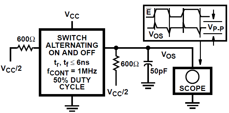 Figure 15-4 Control-To-Switch
Feedthrough Noise Test Circuit
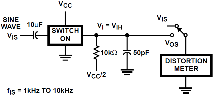 Figure 15-3 Total Harmonic Distortion
Test Circuit
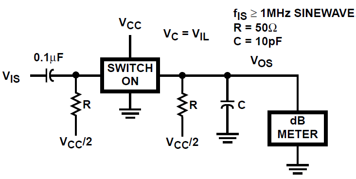 Figure 15-5 Switch Off Signal
Feedthrough
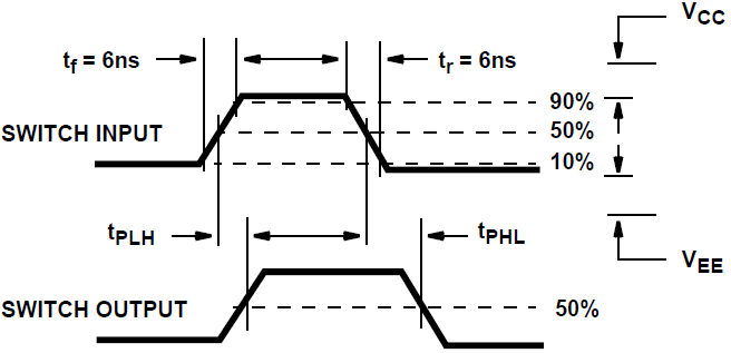 Figure 15-6 Switch Propagation Delay
Times
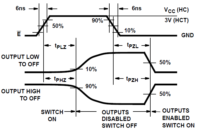 Figure 15-7 Switch Turn-On and
Turn-Off Propagation Delay Times Waveforms