SCHS156D February 1998 – November 2021 CD54HC165 , CD54HCT165 , CD74HC165 , CD74HCT165
PRODUCTION DATA
- 1 Features
- 2 Description
- 3 Revision History
- 4 Pin Configuration and Functions
- 5 Specifications
- 6 Parameter Measurement Information
- 7 Detailed Description
- 8 Power Supply Recommendations
- 9 Layout
- 10Device and Documentation Support
- 11Mechanical, Packaging, and Orderable Information
Package Options
Refer to the PDF data sheet for device specific package drawings
Mechanical Data (Package|Pins)
- N|16
- D|16
Thermal pad, mechanical data (Package|Pins)
Orderable Information
2 Description
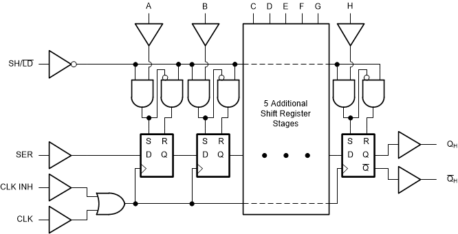
The ’HC165 and ’HCT165 are 8-bit parallel or serial-in shift registers with complementary serial outputs (QH and QH) available from the last stage. When the parallel load (SH/LD) input is LOW, parallel data from the A to H inputs are loaded into the register asynchronously. When the SH/LD is HIGH, data enters the register serially at the SER input and shifts one place to the right (A→B→C, etc.) with each positive-going clock transition. This feature allows parallel-to-serial converter expansion by connecting the QH output to the SER input of the succeeding device.
| PART NUMBER | PACKAGE(1) | BODY SIZE (NOM) |
|---|---|---|
| CD54HC165F3A | CDIP (16) | 24.38 mm × 6.92 mm |
| CD74HC165M | SOIC (16) | 9.90 mm × 3.90 mm |
| CD74HC165E | PDIP (16) | 19.31 mm × 6.35 mm |
| CD54HCT165F3A | CDIP (16) | 24.38 mm × 6.92 mm |
| CD74HCT165M | SOIC (16) | 9.90 mm × 3.90 mm |
| CD74HCT165E | PDIP (16) | 19.31 mm × 6.35 mm |
 Functional
Diagram