SCHS157D February 1998 – February 2022 CD54HC166 , CD54HCT166 , CD74HC166 , CD74HCT166
PRODUCTION DATA
- 1 Features
- 2 Description
- 3 Revision History
- 4 Pin Configuration and Functions
- 5 Specifications
- 6 Parameter Measurement Information
- 7 Detailed Description
- 8 Power Supply Recommendations
- 9 Layout
- 10Device and Documentation Support
- 11Mechanical, Packaging, and Orderable Information
Package Options
Refer to the PDF data sheet for device specific package drawings
Mechanical Data (Package|Pins)
- N|16
- D|16
Thermal pad, mechanical data (Package|Pins)
Orderable Information
2 Description
The ’HC166 and ’HCT166 8-bit shift register is fabricated with silicon gate CMOS technology. It possesses the low power consumption of standard CMOS integrated circuits, and can operate at speeds comparable to the equivalent low power Schottky device.
Device
Information
| PART NUMBER | PACKAGE(1) | BODY SIZE (NOM) |
|---|---|---|
| CD54HC166F3A | CDIP (16) | 24.38 mm × 6.92 mm |
| CD54HCT166F3A | CDIP (16) | 24.38 mm × 6.92 mm |
| CD74HC166M | SOIC (16) | 9.90 mm × 3.90 mm |
| CD74HCT166M | SOIC (16) | 9.90 mm × 3.90 mm |
| CD74HC166E | PDIP (16) | 19.31 mm × 6.35 mm |
| CD74HCT166E | PDIP (16) | 19.31 mm × 6.35 mm |
(1) For all
available packages, see the orderable addendum at
the end of the data sheet.
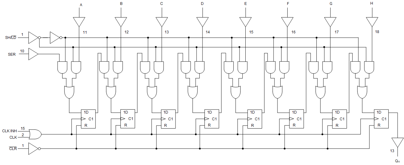
 Functional
Diagram