SCHS208E February 1998 – July 2024 CD54HC4066 , CD74HC4066 , CD74HCT4066
PRODUCTION DATA
- 1
- 1 Features
- 2 Applications
- 3 Description
- 4 Pin Configuration and Functions
- 5 Absolute Maximum Ratings
- 6 ESD Ratings
- 7 Thermal Information
- 8 Recommended Operating Conditions
- 9 Electrical Characteristics: HC Devices
- 10Electrical Characteristics: HCT Devices
- 11Switching Characteristics HC
- 12Switching Characteristics HCT
- 13Analog Channel Specifications
- 14Analog Test Circuits
- 15Test Circuits and Waveforms
- 16Detailed Description
- 17Device and Documentation Support
- 18Revision History
- 19Mechanical, Packaging, and Orderable Information
Package Options
Mechanical Data (Package|Pins)
Thermal pad, mechanical data (Package|Pins)
Orderable Information
3 Description
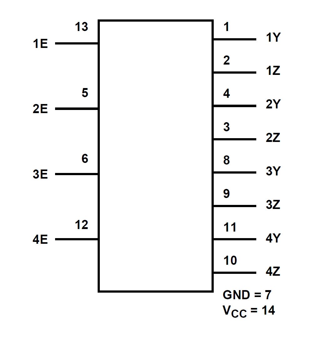
The ’HC4066 and CD74HCT4066 devices contain four independent digitally controlled analog switches that use silicon-gate CMOS technology to achieve operating speeds similar to LSTTL with the low power consumption of standard CMOS integrated circuits.
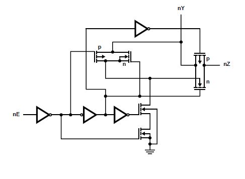
These switches feature the characteristic linear ON resistance of the metal-gate CD4066B device. Each switch is turned on by a high-level voltage on its control input.
Device Information
| PART NUMBER | TEMP. RANGE (°C) | PACKAGE(1) |
|---|---|---|
| CD74HC4066 | -55 to 125 | D (SOIC, 14) |
| -55 to 125 | PW (TSSOP, 14) | |
| CD74HCT4066 | -55 to 125 | D (SOIC, 14) |
(1) For more information, see Section 19.
 Functional Block
Diagram
 Logic Diagram