SCHS209D November 1998 – December 2024 CD74HC4067 , CD74HCT4067
PRODUCTION DATA
- 1
- 1 Features
- 2 Applications
- 3 Description
- 4 Pin Configuration and Functions
- 5 Absolute Maximum Ratings
- 6 Thermal Information
- 7 Recommended Operating Conditions
- 8 Electrical Characteristics: HC Devices
- 9 Electrical Characteristics: HCT Devices
- 10HTC Input Loading
- 11Switching Characteristics HC
- 12Switching Characteristics HCT
- 13Analog Channel Specifications
- 14Typical Characteristics
- 15Analog Test Circuits
- 16Device and Documentation Support
- 17Revision History
- 18Mechanical, Packaging, and Orderable Information
Package Options
Refer to the PDF data sheet for device specific package drawings
Mechanical Data (Package|Pins)
- DW|24
Thermal pad, mechanical data (Package|Pins)
- DW|24
Orderable Information
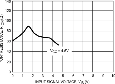
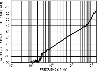
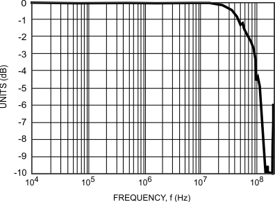
14 Typical Characteristics

| TA = 25°C | GND = 0 V | |||

| VCC = 4.5 V | RL = 50 Ω | TA = 25°C | ||

| VCC = 4.5 V | RL = 50 Ω | TA = 25°C |