SCHS212E February 1998 – July 2024 CD54HC4316 , CD74HC4316 , CD74HCT4316
PRODUCTION DATA
- 1
- 1 Features
- 2 Description
- 3 Pin Configurations and Functions
- 4 Absolute Maximum Ratings
- 5 Thermal Information
- 6 Recommended Operating Conditions
- 7 Electrical Characteristics: HC Devices
- 8 Electrical Characteristics: HCT Devices
- 9 Switching Characteristics HC
- 10Switching Characteristics HCT
- 11Analog Channel Specifications
- 12HCT Input Loading Table
- 13Recommended Operating Area as a Function of Supply Voltage
- 14Typical Performance Curves
- 15Parameter Measurement Information
- 16Detailed Description
- 17Device and Documentation Support
- 18Revision History
- 19Mechanical, Packaging, and Orderable Information
Package Options
Refer to the PDF data sheet for device specific package drawings
Mechanical Data (Package|Pins)
- N|16
- D|16
Thermal pad, mechanical data (Package|Pins)
- D|16
Orderable Information
3 Pin Configurations and Functions
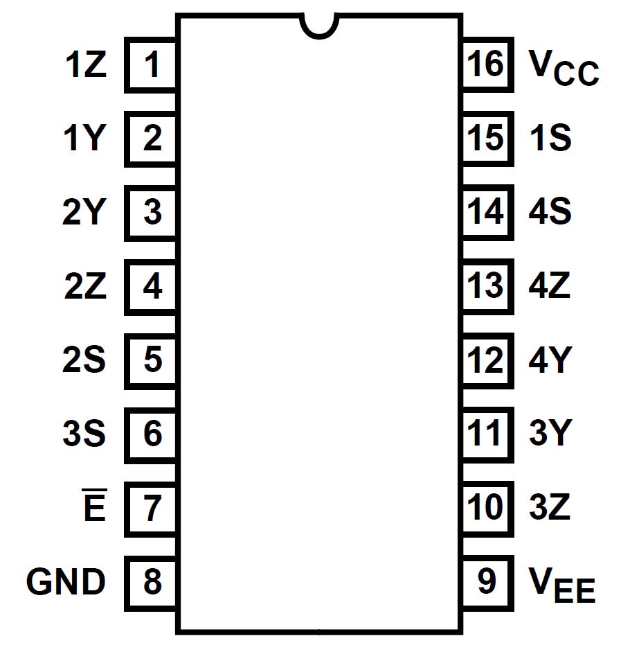
 Figure 3-1 CD74HC4316 (TSSOP)
Table 3-1 Pin Functions
| PIN | TYPE | DESCRIPTION | |
|---|---|---|---|
| NAME | NO. | ||
| 1Z | 1 | I/O | Input/Output for Switch 1 |
| 1Y | 2 | I/O | Input/Output for Switch 1 |
| 2Y | 3 | I/O | Input/Output for Switch 2 |
| 2Z | 4 | I/O | Input/Output for Switch 2 |
| 2S | 5 | I | Control pin for Switch 2 |
| 3S | 6 | I | Control pin for Switch 3 |
| E | 7 | I | Enable Pin |
| GND | 8 | - | Ground Pin |
| VEE | 9 | - | Power Pin |
| 3Z | 10 | I/O | Input/Output for Switch 3 |
| 3Y | 11 | I/O | Input/Output for Switch 3 |
| 4Y | 12 | I/O | Input/Output for Switch 4 |
| 4Z | 13 | I/O | Input/Output for Switch 4 |
| 4S | 14 | I | Control pin for Switch 4 |
| 1S | 15 | I | Control pin for Switch 1 |
| VCC | 16 | - | Power Pin |