SCLS455E February 2001 – June 2022 CD54HCT573 , CD74HCT573
PRODUCTION DATA
- 1 Features
- 2 Description
- 3 Revision History
- 4 Pin Configuration and Functions
- 5 Specifications
- 6 Parameter Measurement Information
- 7 Detailed Description
- 8 Power Supply Recommendations
- 9 Layout
- 10Device and Documentation Support
- 11Mechanical, Packaging, and Orderable Information
Package Options
Refer to the PDF data sheet for device specific package drawings
Mechanical Data (Package|Pins)
- DB|20
- N|20
- DW|20
Thermal pad, mechanical data (Package|Pins)
Orderable Information
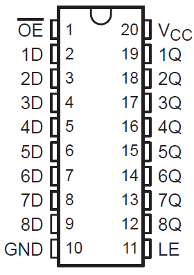
4 Pin Configuration and Functions
 J, DB, N, or DW Package
20-Pin CDIP, SSOP, PDIP, SOIC
Top View