SCHS138D November 1998 – March 2022 CD74HC93 , CD74HCT93
PRODUCTION DATA
- 1 Features
- 2 Description
- 3 Revision History
- 4 Pin Configuration and Functions
- 5 Specifications
- 6 Parameter Measurement Information
- 7 Detailed Description
- 8 Power Supply Recommendations
- 9 Layout
- 10Device and Documentation Support
- 11Mechanical, Packaging, and Orderable Information
Package Options
Refer to the PDF data sheet for device specific package drawings
Mechanical Data (Package|Pins)
- N|14
Thermal pad, mechanical data (Package|Pins)
Orderable Information
2 Description
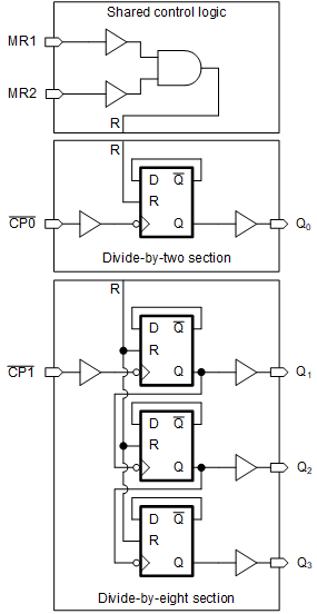
The CD74HC93 and CD74HCT93 are high-speed silicon-gate CMOS devices and are pin-compatible with low power Schottky TTL (LSTTL). These 4-bit binary ripple counters consist of four flip-flops internally connected to provide a divide-by-two section and a divide-by-eight section. Each section has a separate clock input (CP0 and CP1) to initiate state changes of the counter on the HIGH to LOW clock transition. State changes of the Qn outputs do not occur simultaneously because of internal ripple delays. Therefore, decoded output signals are subject to decoding spikes and should not be used for clocks or strobes.
| PART NUMBER | PACKAGE(1) | BODY SIZE (NOM) |
|---|---|---|
| CD74HC93M | SOIC (14) | 8.65 mm × 3.90 mm |
| CD74HC93E | PDIP (14) | 19.31 mm × 6.35 mm |
| CD74HCT93E | PDIP (14) | 19.31 mm × 6.35 mm |
 Functional Block
Diagram