SCHS371H
November 2009 – October 2024
CDC3RL02
PRODUCTION DATA
1
1
Features
2
Applications
3
Description
4
Device Comparison
5
Pin Configuration and Functions
6
Specifications
6.1
Absolute Maximum Ratings
6.2
ESD Ratings
6.3
Recommended Operating Conditions
6.4
Thermal Information
6.5
Electrical Characteristics
6.6
Typical Characteristics
7
Detailed Description
7.1
Overview
7.2
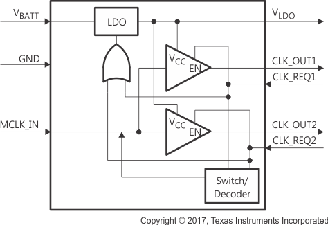
Functional Block Diagram
7.3
Feature Description
7.3.1
Low Additive Noise
7.3.2
Regulated 1.8V Externally Available I/O Supply
7.3.3
Ultra-Small 8-bump YFP 0.4mm Pitch WCSP Package
7.4
Device Functional Modes
8
Application and Implementation
8.1
Application Information
8.1.1
Input Clock Squarer
8.1.2
Output Stage
8.1.3
LDO
8.2
Typical Application
8.2.1
Design Requirements
8.2.2
Detailed Design Procedure
8.2.3
Application Curve
8.3
Power Supply Recommendations
8.4
Layout
8.4.1
Layout Guidelines
8.4.2
Layout Example
9
Device and Documentation Support
9.1
Documentation Support
9.1.1
Related Documentation
9.2
Receiving Notification of Documentation Updates
9.3
Support Resources
9.4
Trademarks
9.5
Electrostatic Discharge Caution
9.6
Glossary
10
Revision History
11
Mechanical, Packaging, and Orderable Information
Package Options
Mechanical Data (Package|Pins)
YFP|8
MXBG057R
Thermal pad, mechanical data (Package|Pins)
Orderable Information
schs371h_oa
schs371h_pm
2
Applications
Cellular Phones
Global Positioning Systems (GPS)
Wireless LAN
FM Radio
WiMAX
W-BT
Simplified Block Diagram