SNAS833A November   2021  – May 2022 CDCDB400

PRODUCTION DATA  

  1. Features
  2. Applications
  3. Description
  4. Revision History
  5. Pin Configuration and Functions
  6. Specifications
    1. 6.1 Absolute Maximum Ratings
    2. 6.2 ESD Ratings
    3. 6.3 Recommended Operating Conditions
    4. 6.4 Thermal Information
    5. 6.5 Electrical Characteristics
    6. 6.6 Timing Requirements
    7. 6.7 Typical Characteristics
  7. Parameter Measurement Information
  8. Detailed Description
    1. 8.1 Overview
    2. 8.2 Functional Block Diagram
    3. 8.3 Feature Description
      1. 8.3.1 Fail-Safe Input
      2. 8.3.2 Output Enable Control
      3. 8.3.3 SMBus
        1. 8.3.3.1 SMBus Address Assignment
    4. 8.4 Device Functional Modes
      1. 8.4.1 CKPWRGD_PD# Function
      2. 8.4.2 OE[3:0]# and SMBus Output Enables
      3. 8.4.3 Output Slew Rate Control
      4. 8.4.4 Output Impedance Control
    5. 8.5 Programming
    6. 8.6 Register Maps
      1. 8.6.1 CDCDB400 Registers
  9. Application and Implementation
    1. 9.1 Application Information
    2. 9.2 Typical Application
      1. 9.2.1 Design Requirements
      2. 9.2.2 Detailed Design Procedure
        1. 9.2.2.1 Output Enable Control Method
        2. 9.2.2.2 SMBus Address
      3. 9.2.3 Application Curves
  10. 10Power Supply Recommendations
  11. 11Layout
    1. 11.1 Layout Guidelines
    2. 11.2 Layout Examples
  12. 12Device and Documentation Support
    1. 12.1 Device Support
      1. 12.1.1 TICS Pro
    2. 12.2 Receiving Notification of Documentation Updates
    3. 12.3 Support Resources
    4. 12.4 Trademarks
    5. 12.5 Electrostatic Discharge Caution
    6. 12.6 Glossary
  13. 13Mechanical, Packaging, and Orderable Information

Package Options

Mechanical Data (Package|Pins)
Thermal pad, mechanical data (Package|Pins)
Orderable Information

Application Curves

Figure 6-1 in the Typical Characteristics section can be used as both an application curve and a typical characteristics plot in this example.

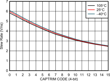
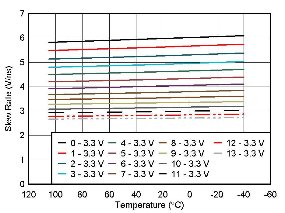
The Figure 9-2 and Figure 9-3 show characterization data for the Output slew rate for various CAPTRIM codes and across temperature. Customers can use these plots as reference for choosing the appropriate output slew rate based on their system requirement.
GUID-20210519-CA0I-NCDV-T6D0-XQBVPWQS87VF-low.gif
Figure 9-2 Output Slew Rate vs. CAPTRIM Code
GUID-20210519-CA0I-TMG0-4CL3-WT58FSFVT3B9-low.gif
Figure 9-3 Slew Rate Variation Across Temperature for Different CAPTRIM Code