SNAS818B July   2021  – May 2022 CDCDB800

PRODUCTION DATA  

  1. Features
  2. Applications
  3. Description
  4. Revision History
  5. Pin Configuration and Functions
  6. Specifications
    1. 6.1 Absolute Maximum Ratings
    2. 6.2 ESD Ratings
    3. 6.3 Recommended Operating Conditions
    4. 6.4 Thermal Information
    5. 6.5 Electrical Characteristics
    6. 6.6 Timing Requirements
    7. 6.7 Typical Characteristics
  7. Parameter Measurement Information
  8. Detailed Description
    1. 8.1 Overview
    2. 8.2 Functional Block Diagram
    3. 8.3 Feature Description
      1. 8.3.1 Fail-Safe Input
      2. 8.3.2 Output Enable Control
      3. 8.3.3 SMBus
        1. 8.3.3.1 SMBus Address Assignment
    4. 8.4 Device Functional Modes
      1. 8.4.1 CKPWRGD_PD# Function
      2. 8.4.2 OE[7:0]# and SMBus Output Enables
      3. 8.4.3 Output Slew Rate Control
      4. 8.4.4 Output Impedance Control
    5. 8.5 Programming
    6. 8.6 Register Maps
      1. 8.6.1 CDCDB800 Registers
  9. Application and Implementation
    1. 9.1 Application Information
    2. 9.2 Typical Application
      1. 9.2.1 Design Requirements
      2. 9.2.2 Detailed Design Procedure
        1. 9.2.2.1 Output Enable Control Method
      3. 9.2.3 Application Curves
  10. 10Power Supply Recommendations
  11. 11Layout
    1. 11.1 Layout Guidelines
    2. 11.2 Layout Examples
  12. 12Device and Documentation Support
    1. 12.1 Device Support
      1. 12.1.1 TICS Pro
    2. 12.2 Receiving Notification of Documentation Updates
    3. 12.3 Support Resources
    4. 12.4 Trademarks
    5. 12.5 Electrostatic Discharge Caution
    6. 12.6 Glossary
  13. 13Mechanical, Packaging, and Orderable Information

Package Options

Mechanical Data (Package|Pins)
Thermal pad, mechanical data (Package|Pins)
Orderable Information

Typical Characteristics

Figure 6-1 shows both the phase noise of the source as well as the output of the DUT (CDCDB800). It can be seen from the phase noise plot that the DUT has a very low phase noise profile with total jitter of 71 fs, rms. If we rms subtract the clock reference noise, the additive jitter of CDCDB800 under typical conditions would be lower than 71 fs, rms.
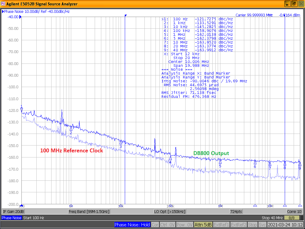
GUID-20210608-CA0I-FDGZ-RWL2-K1C7GKWM7P1Q-low.png Figure 6-1 CDCDB800 Clock Out (CK0:8) Phase Noise