SNAS820A August   2021  – May 2022 CDCDB803

PRODUCTION DATA  

  1. Features
  2. Applications
  3. Description
  4. Revision History
  5. Pin Configuration and Functions
  6. Specifications
    1. 6.1 Absolute Maximum Ratings
    2. 6.2 ESD Ratings
    3. 6.3 Recommended Operating Conditions
    4. 6.4 Thermal Information
    5. 6.5 Electrical Characteristics
    6. 6.6 Timing Requirements
    7. 6.7 Typical Characteristics
  7. Parameter Measurement Information
  8. Detailed Description
    1. 8.1 Overview
    2. 8.2 Functional Block Diagram
    3. 8.3 Feature Description
      1. 8.3.1 Fail-Safe Input
      2. 8.3.2 Output Enable Control
      3. 8.3.3 SMBus
        1. 8.3.3.1 SMBus Address Assignment
    4. 8.4 Device Functional Modes
      1. 8.4.1 CKPWRGD_PD# Function
      2. 8.4.2 OE[7:0]# and SMBus Output Enables
      3. 8.4.3 Output Slew Rate Control
      4. 8.4.4 Output Impedance Control
    5. 8.5 Programming
    6. 8.6 Register Maps
      1. 8.6.1 CDCDB803 Registers
  9. Application and Implementation
    1. 9.1 Application Information
    2. 9.2 Typical Application
      1. 9.2.1 Design Requirements
      2. 9.2.2 Detailed Design Procedure
        1. 9.2.2.1 Output Enable Control Method
        2. 9.2.2.2 SMBus Address
      3. 9.2.3 Application Curves
  10. 10Power Supply Recommendations
  11. 11Layout
    1. 11.1 Layout Guidelines
    2. 11.2 Layout Examples
  12. 12Device and Documentation Support
    1. 12.1 Device Support
      1. 12.1.1 TICS Pro
    2. 12.2 Receiving Notification of Documentation Updates
    3. 12.3 Support Resources
    4. 12.4 Trademarks
    5. 12.5 Electrostatic Discharge Caution
    6. 12.6 Glossary
  13. 13Mechanical, Packaging, and Orderable Information

Package Options

Mechanical Data (Package|Pins)
Thermal pad, mechanical data (Package|Pins)
Orderable Information

Typical Application

Figure 9-1 shows a CDCDB803 typical application. In this application, a clock generator provides a 100-MHz reference to the CDCDB803 which then distributes that clock to PCIe endpoints. The clock generator may be a discrete clock generator like the CDCI6214 or it may be integrated in a larger component such as a Platform Controller Hub (PCH) or application processor.
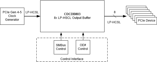
GUID-20210112-CA0I-MD7B-6LBH-S9QZ5VSHBNSK-low.gif Figure 9-1 Typical Application