-
CDCE62002 Four Output Clock Generator/Jitter Cleaner With Integrated Dual VCOs
- 1 Features
- 2 Applications
- 3 Description
- 4 Revision History
- 5 Description (continued)
- 6 Pin Configuration and Functions
- 7 Specifications
- 8 Parameter Measurement Information
-
9 Detailed Description
- 9.1 Overview
- 9.2 Functional Block Diagrams
- 9.3
Feature Description
- 9.3.1 Phase Noise Analysis
- 9.3.2 Output-to-Output Isolationthe OUTPUT TO OUTPUT ISOLATION section
- 9.3.3 Device Control
- 9.3.4 External Control Pins
- 9.3.5 Input Block
- 9.3.6 Lock Detect
- 9.3.7 Crystal Input Interface
- 9.3.8 VCO Calibration
- 9.3.9 Start-Up Time Estimation
- 9.4 Device Functional Modes
- 9.5 Programming
- 9.6 Register Maps
- 10Power Supply Recommendations
- 11Layout
- 12Device and Documentation Support
- 13Mechanical, Packaging, and Orderable Information
- IMPORTANT NOTICE
Package Options
Mechanical Data (Package|Pins)
- RHB|32
Thermal pad, mechanical data (Package|Pins)
- RHB|32
Orderable Information
CDCE62002 Four Output Clock Generator/Jitter Cleaner With Integrated Dual VCOs
1 Features
- Frequency Synthesizer With PLL/VCO and Partially Integrated Loop Filter
- Fully Configurable Outputs Including Frequency and Output Format
- Smart Input Multiplexer Automatically Switches Between One of Two Reference Inputs
- Multiple Operational Modes Include Clock Generation Through Crystal, SERDES Start-Up Mode, Jitter Cleaning, and Oscillator Based Holdover Mode
- Integrated EEPROM Determines Device Configuration at Power Up
- Excellent Jitter Performance
- Integrated Frequency Synthesizer Including PLL, Multiple VCOs, and Loop Filter:
- Full Programmability Facilitates Phase Noise Performance Optimization Enabling Jitter Cleaner Mode
- Programmable Charge Pump Gain and Loop Filter Settings
- Unique Dual-VCO Architecture Supports a Wide Tuning Range 1.750 GHz to 2.356 GHz.
- Universal Output Blocks Support Up to 2 Differential, 4 Single-Ended, or Combinations of Differential or Single-Ended:
- 0.5 ps RMS (10 kHz to 20 MHz) Output Jitter Performance
- Low Output Phase Noise: –130 dBc/Hz at 1 MHz Offset, Fc = 491.52 MHz
- Output Frequency Ranges From 10.94 MHz to 1.175 GHz in Synthesizer Mode
- LVPECL, LVDS, and LVCMOS
- Independent Output Dividers Support Divide Ratios for 1, 2, 3, 4, 5, 8, 10, 12, 16, 20, 24, and 32
- Flexible Inputs With Innovative Smart Multiplexer:
- Two Universal Differential Inputs Accept Frequencies from 1 MHz up to 500 MHz (LVPECL), 500 MHz (LVDS), or 250 MHz (LVCMOS)
- One Auxiliary Input Accepts Crystals in the Range of 2 MHz to 42 MHz
- Clock Generator Mode Using Crystal Input
- Smart Input Multiplexer Can be Configured to Automatically Switch Between Highest Priority Clock Source Available Allowing for Fail-Safe Operation
- Typical Power Consumption 750 mW at 3.3 V
- Integrated EEPROM Stores Default Settings; Therefore, the Device Can Power Up in a Known, Predefined State
- Offered in QFN-32 Package
- ESD Protection Exceeds 2000 V HBM
- Industrial Temperature Range: –40°C to +85°C
2 Applications
- Data Converter and Data Aggregation Clocking
- Wireless Infrastructure
- Switches and Routers
- Medical Electronics
- Military and Aerospace
- Industrial
- Clock Generation and Jitter Cleaning
3 Description
The CDCE62002 device is a high-performance clock generator featuring low output jitter, a high degree of configurability through a SPI interface, and programmable start-up modes determined by on-chip EEPROM. Specifically tailored for clocking data converters and high-speed digital signals, the CDCE62002 achieves jitter performance under 0.5 ps RMS (1).
Device Information(1)
| PART NUMBER | PACKAGE | BODY SIZE (NOM) |
|---|---|---|
| CDCE62002 | VQFN (32) | 5.00 mm × 5.00 mm |
- For all available packages, see the orderable addendum at the end of the data sheet.
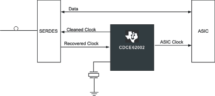
CDCE62002 Application Example
4 Revision History
Changes from D Revision (February 2012) to E Revision
- Added figure cross references to Electrical TablesGo
- Added figure titles.Go
- Updated Figure 18Go
- Updated Figure 20Go
- Corrected description for bits 0 and 1 in CDCE62002 Register 0 Bit Definitions Go
- Corrected the register bits for LVPECL-AC, LVPECL-DC, LVDS-AC, LVDS-DC reference inputs in Reference Input AC/DC Input Termination Table Go
Changes from C Revision (March 2011) to D Revision
- Added 3 rows in TIMING REQUIREMENTS table, under Duty Cycle rowGo
- Added a sentence below Equation 3Go
- Changed last row last column in Figure 23 truth table from Disabled to Input Buffer Termination DisabledGo
- Changed in Table 13, second column, 5th and 6th row from 1 to 0Go
- Added a reference to Table 11 and 2 references to Table 12 in Table 6Go
- Added 6 crossreferences to Table 8 Go
- Changed changed last row in Table 8 Description column, from "always reads 1" to "May read back to 1 or 0"Go
Changes from B Revision (February 2010) to C Revision
- Changed the description of Pin 30, REF_IN-.Go
- Changed Pin 7 to open drain in Pin Functions tableGo
- Changed the description of Pin 19, TESTSYNC To: Reserved Pin.....resistor.Go
- Changed pin 31 From: Power To: A. Power in Pin Functions tableGo
- Changed Pin Functions table, Pins 9, 12 to VCC_OUT0. Pins 13 and 16 to VCC_OUT1Go
- Changed Note1 of the Pin Functions tableGo
- Deleted Dividers and from ELEC CHARACTERISTICS table in row POFFGo
- Changed Crytal input section first row From: Crystal Load Capacitance To: On-chip Load CapacitanceGo
- Added SPI OUTPUT row From: PLL To: PLL_LOCKGo
- Changed tr / tf Max value From: 735 To: 135Go
- Deleted (Reg 0 RAM bit 9 = 1) and (Reg 0 RAM bit 9 = 0) from the TIMING REQUIREMENTS table Go
- Added Driver Level and Max shunt capacitance to AUXILARY_IN REQUIREMENT in the TIMING REQUIREMENTS tableGo
- Deleted Columns from Table 1: LVDS-HP and LVCMOS-HPGo
- Changed Table 2 Go
- Changed the OUTPUT TO OUTPUT ISOLATION sectionGo
- Deleted the SPI CONTROL INTERFACE TIMING sectionGo
- Updated Figure 18Go
- Updated Reference Input Buffer Go
- Updated Figure 20Go
- Changed the Smart Multiplexer Dividers sectionGo
- Changed Changed the text in the Smart Multiplexer Divider sectionGo
- Changed Figure 24Go
- Deleted column 3 db Corner C3R3 from Table 12Go
- Added sections: VCO Calibration, Crystal Input Interface, and Startup TimeGo
- Changed Figure 29Go
- Changed the INTERFACE AND CONTROL BLOCK sectionGo
- Changed figure Figure 36Go
- Changed Table 17, RAM BITS To REGISTER BITSGo
- Deleted the First four rows in Table 18 and the first columnGo
- Deleted (6 settings+DisAble+Enable) in Register bit 19 of Table 18Go
- Added ; set '0' to TI use Only in bit 26 in Table 18Go
- Changed the description of bit 27 in Table 18Go
- Deleted the First four rows in Table 19 and the first columnGo
- Added Receiving Notification of Documentation Updates section Go
Changes from A Revision (July, 2009) to B Revision
- Deleted feature reference to Single Ended Clock Source or Crystal and LVCMOS Input of up to 75 MHz Go
- Deleted references to single ended inputs and CMOS clock from description.Go
- Changed the description of Pin 2, AUX_INGo
- Deleted LVCMOS INPUT MODE (AUX_IN) section from Electrical CharacteristicsGo
- Changed Crystal Shunt Capacitance to Crystal Load Capacitance with a MIN value of 8Go
- Deleted fREF – Single paramter from AUXILARY_IN_REQUIRMENTSGo
- Deleted references to EEPROM Locking from "Interface and Control Block" sectionGo
- Changed Auxiliary Input Port sectionGo
- Deleted External Feed Back Mode sectionGo
- Deleted External Feedback Option sectionGo
- Changed EXTFEEDBACK to RESERVED for bit 10 in Table 16Go
- Changed EELOCK to RESERVED for bit 30 in Table 18Go
Changes from * Revision (June 2009) to A Revision
- Added information to Pin 18 description - The input has an internal 150-kΩ pull-up resistGo
- Added NOTE: All VCC pins need to be connected for the device to operate properly.Go
- Changed PLVPECL, PLVDS, PLVCMOS and POFF Unit values From: W To: mWGo
- Deleted underscore before IN+Go
- Deleted 6 from 8006Go
- Changed Y4 to Y1Go
- Added tr / tf MIN, TYP, and MAX valuesGo
- Added (Reg 0 RAM bit 9 = 0) to fREF – Diff REF_DIV Go
- Changed graphic input namingGo
- Changed graphic input namingGo
- Changed REF into REF_INGo
- Changed graphicGo
- Changed Table 4Go
- Changed PDDRESET to PLLRESET, in Table 4Go
- Changed Power_Down to PD, in Table 4Go
- Changed PRI_IN to REF_IN in Figure 19Go
- Changed PRI_IN to REF_INGo
- Changed PRI_IN to REF_INGo
- Changed part number errorGo
- Changed REFERENCE to REF_IN and AUXILARY to AUX_IN, Table 16Go
- Changed power to currentGo
- Changed the description of bits 0 - 5 To: TI Test Registers. For TI Use Only in Table 19Go
5 Description (continued)
It incorporates a synthesizer block with partially integrated loop filter, a clock distribution block including programmable output formats, and an input block featuring an innovative smart multiplexer. The clock distribution block includes two individually programmable outputs that can be configured to provide different combinations of output formats (LVPECL, LVDS, LVCMOS). Each output can also be programmed to a unique output frequency (ranging from 10.94 MHz to 1.175 GHz (1)). If Both outputs are configured in single-ended mode (such as LVCMOS), the CDCE62002 supports up to four outputs. The input block includes one universal differential inputs which support frequencies up to 500 MHz and an auxiliary input that can be configured to connect to an external AT-Cut crystal through an onboard oscillator block. The smart input multiplexer has two modes of operation, manual and automatic. In manual mode, the user selects the synthesizer reference through the SPI interface. In automatic mode, the input multiplexer will automatically select between the highest priority input clock available.
6 Pin Configuration and Functions
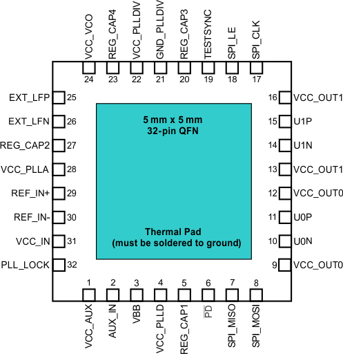
Pin Functions
| PIN | TYPE | DESCRIPTION(1) | |
|---|---|---|---|
| NAME | NO. | ||
| AUX_IN | 2 | I | Auxiliary Input is a Crystal input pin that connect to an internal oscillator circuitry. |
| EXT_LFN | 26 | Analog | External Loop Filter Input Negative. |
| EXT_LFP | 25 | Analog | External Loop Filter Input Positive |
| GND | PAD | Ground | Ground is on Thermal PAD. See Layout Guidelines |
| GND_PLLDIV | 21 | Ground | Ground for PLL Divider circuitry. (short to GND) |
| PD | 6 | I | PD or Power-Down Pin is an active low pin and can be activated externally or through the corresponding Bit in SPI Register 2 While PD is asserted (low), the device is shut down. When PD switches high the EEPROM becomes loaded into the RAM. After the selected input clock signal becomes available, the VCO starts calibration and the PLL aims to achieve lock. All Output dividers become initiated. During self-calibration, the outputs are held static (for example, logical zero). PD pin has an internal 150-kΩ pullup resistor. Note: The SPI_LE signal has to be high in order for the EEPROM to load correctly into RAM on the Rising edge of PD. |
| PLL_LOCK | 32 | O | PLL Lock indicator |
| REF_IN+ | 29 | I | Universal Input Buffer (LVPECL, LVDS, LVCMOS) positive input for the Reference Clock. |
| REF_IN– | 30 | I | Universal Input Buffer (LVPECL, LVDS,) negative input for the Reference Clock. This pin must be pulled to ground through 1-kΩ resistor when input is selected LVCMOS. |
| REG_CAP1 | 5 | Analog | Capacitor for the internal Regulator. Connect to a 10-μF Capacitor (Y5V) |
| REG_CAP2 | 27 | Analog | Capacitor for the internal Regulator. Connect to a 10-μF Capacitor (Y5V) |
| REG_CAP3 | 20 | Analog | Capacitor for the internal Regulator. Connect to a 10-μF Capacitor (Y5V) |
| REG_CAP4 | 23 | Analog | Capacitor for the internal Regulator. Connect to a 10-μF Capacitor (Y5V) |
| SPI_CLK | 17 | I | LVCMOS input, serial Control Clock Input for the SPI bus interface, with Hysteresis. |
| SPI_LE | 18 | I | LVCMOS input, control Latch Enable for Serial Programmable Interface. Note: The SPI_LE signal has to be high in order for the EEPROM to load correctly on the Rising edge of PD. The input has an internal 150-kΩ pull-up resistor |
| SPI_MISO | 7 | O | 3-state LVCMOS Output that is enabled when SPI_LE is asserted low. It is the serial Data Output to the SPI bus interface. |
| SPI_MOSI | 8 | I | LVCMOS input, Master Out Slave In as a serial Control Data Input to CDCE62002 for the SPI bus interface. |
| TESTSYNC | 19 | I | Reserved Pin. Pull this pin down to ground using 1-kΩ resistor. |
| U0P:U0N U1P:U1N |
11,10 15,14 |
O | The outputs of CDCE62002 are user definable and can be any combination of up to 2 LVPECL outputs, 2 LVDS outputs or up to 4 LVCMOS outputs. The outputs are selectable through SPI interface. The power-up setting is EEPROM configurable. |
| VBB | 3 | Analog | Capacitor for the internal termination Voltage. Connect to a 1-μF Capacitor (Y5V) |
| VCC_AUX | 1 | A. Power | 3.3-V Supply Power for Crystal/Auxiliary Input Buffer Circuitry |
| VCC_IN | 31 | A. Power | 3.3-V Supply Power for Input Buffer Circuitry |
| VCC_OUT0 | 9, 12 | Power | 3.3-V Supply for the Output Buffers. |
| VCC_OUT1 | 13, 16 | ||
| VCC_PLLA | 28 | A. Power | 3.3-V Supply Power for the PLL circuitry. |
| VCC_PLLD | 4 | Power | 3.3-V Supply Power for the PLL circuitry. |
| VCC_PLLDIV | 22 | Power | 3.3-V Supply Power for the PLL circuitry. |
| VCC_VCO | 24 | A. Power | 3.3-V Supply Power for the VCO circuitry. |
VCC_PLLA + VCC_VCO
VCC_PLLD + VCC_PLLDIV
VCC_IN + VCC_AUXIN
VCC_OUT0 + VCC_OUT1
All VCC pins need to be connected for the device to operate properly.
7 Specifications
7.1 Absolute Maximum Ratings
over operating free-air temperature range (unless otherwise noted) (1)| MIN | MAX | UNIT | ||
|---|---|---|---|---|
| Supply voltage VCC(2) | –0.5 | V | ||
| Input voltage, VI (3) | –0.5 | V | ||
| Output voltage, VO (3) | –0.5 | V | ||
| Input current (VI < 0, VI > VCC) | ±20 | mA | ||
| Output current for LVPECL/LVCMOS Outputs (0 < VO < VCC) | ±50 | mA | ||
| TJ | Junction temperature | 125 | °C | |
| Tstg | Storage temperature | –65 | 150 | °C |
7.2 Thermal Information
| THERMAL METRIC(1) | CDCE62002 | UNIT | ||
|---|---|---|---|---|
| QFN (RGZ) | ||||
| 32 PINS | ||||
| RθJA | Junction-to-ambient thermal resistance (JEDEC Compliant Board - 3×3 vias on pad) | 0-lfm Airflow | 35 | °C/W |
| 200-lfm Airflow | 28.3 | |||
| 400-lfm Airflow | 27.2 | |||
| RθJP | Junction-to-pad | 1.13 | °C/W | |
7.3 Electrical Characteristics
recommended operating conditions for the CDCE62002 Device for under the specified Industrial temperature range of –40°C to 85°C| PARAMETER | TEST CONDITIONS | MIN | TYP(1) | MAX | UNIT | ||
|---|---|---|---|---|---|---|---|
| POWER SUPPLY | |||||||
| Supply voltage, VCC_OUT, VCC_PLLDIV, VCC_PLLD, VCC_IN, and VCC_AUX | 3 | 3.3 | 3.6 | V | |||
| Analog supply voltage, VCC_PLLA, & VCC_VCO | 3 | 3.3 | 3.6 | V | |||
| PLVPECL | REF at 30.72 MHz, outputs are LVPECL | Output 1 = 491.52 MHz
Output 2 = 245.76 MHz In case of LVCMOS Outputs (1) = 245.76MHz |
850 | mW | |||
| PLVDS | REF at 30.72 MHz, outputs are LVDS | 750 | mW | ||||
| PLVCMOS | REF at 30.72 MHz, outputs are LVCMOS | 800 | mW | ||||
| POFF | REF at 30.72 MHz | Outputs are disabled | 450 | mW | |||
| PPD | Device is powered down | 40 | mW | ||||
| DIFFERENTIAL INPUT MODE (REF_IN) | |||||||
| Differental Input amplitude, (VIN+ – VIN–) | 0.1 | 1.3 | V | ||||
| Common-mode input voltage, VIC | 1.0 | VCC–03 | V | ||||
| IIH | Differential input current high (no internal termination) | VI = VCC, VCC = 3.6 V |
20 | μA | |||
| IIL | Differential input current low (no internal termination) | VI = 0 V, VCC = 3.6 V |
–20 | μA | |||
| Input Capacitance on REF_IN | 3 | pF | |||||
| CRYSTAL INPUT SPECIFICATIONS | |||||||
| On-chip load capacitance | 8 | 10 | pF | ||||
| Equivalent Series Resistance (ESR) | 50 | Ω | |||||
| LVCMOS INPUT MODE (SPI_CLK,SPI_MOSI,SPI_LE,PD, REF_IN) | |||||||
| VIL | Low-level input voltage LVCMOS | 0 | 0.3 VCC | V | |||
| VIH | High-level input voltage LVCMOS | 0.7 VCC | VCC | V | |||
| VIK | LVCMOS input clamp voltage | VCC = 3 V, II = –18 mA | –1.2 | V | |||
| IIH | LVCMOS input current VI = | VCC, VCC = 3.6 V | 20 | μA | |||
| IIL | LVCMOS input (Except REF_IN) | VI = 0 V, VCC = 3.6 V | –10 | –40 | μA | ||
| IIL | LVCMOS input (REF_IN) | VI = 0 V, VCC = 3.6 V | –10 | 10 | μA | ||
| CI | Input capacitance (LVCMOS signals) | VI = 0 V or VCC = 3 | 3 | pF | |||
| SPI OUTPUT (MISO) / PLL_LOCK | |||||||
| IOH | High-level output current | VCC = 3.3 V, | VO = 1.65 V | –30 | mA | ||
| IOL | Low-level output current | VCC = 3.3 V, | VO = 1.65 V | 33 | mA | ||
| VOH | High-level output voltage for LVCMOS outputs | VCC = 3 V, | IOH = –100 μA | VCC–0.5 | V | ||
| VOL | Low-level output voltage for LVCMOS outputs | VCC = 3 V, | IOH = 100 μA | 0.3 | V | ||
| CO | Output capacitance o MISO | VCC = 3.3 V; VO = 0 V or VCC | 3 | pF | |||
| IOZH | 3-state output current | VO = VCC, VO = 0 V | 5 | μA | |||
| IOZL | –5 | μA | |||||
| EEPROM | |||||||
| EEcyc | Programming cycle of EEPROM | 100 | 1000 | Cycles | |||
| EEret | Data retention | 10 | Years | ||||
| VBB ( INPUT BUFFER INTERNAL TERMINATION VOLTAGE REFERENCE) | |||||||
| VBB | Input termination voltage | IBB = –0.2 mA, depending on the setting | 1.2 | 1.9 | V | ||
| INPUT BUFFERS INTERNAL TERMINATION RESISTORS (REF_IN) | |||||||
| Termination resistance | Single-ended | 5 | kΩ | ||||
| PHASE DETECTOR | |||||||
| fCPmax | Charge pump frequency | 0.04 | 40 | MHz | |||
| LVCMOS | |||||||
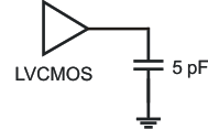
| fclk | Output frequency, see Figure 7 | Load = 5 pF to GND | 250 | MHz | |||
| VOH | High-level output voltage for LVCMOS outputs | VCC = min to max | IOH = –100 μA | VCC–0.5 | V | ||
| VOL | Low-level output voltage for LVCMOS outputs | VCC = min to max | IOL = 100 μA | 0.3 | V | ||
| IOH | High-level output current | VCC = 3.3 V | VO = 1.65 V | –30 | mA | ||
| IOL | Low-level output current | VCC = 3.3 V | VO = 1.65 V | 33 | mA | ||
| tsko | Skew, output to output For Y0 to Y1 | Both outputs set at 122.88 MHz, reference = 30.72 MHz |
75 | ps | |||
| CO | Output capacitance on Y0 to Y1 | VCC = 3.3 V; VO = 0 V or VCC | 5 | pF | |||
| IOZH | Tristate LVCMOS output current | VO = VCC | 5 | μA | |||
| IOZL | Tristate LVCMOS output current | VO = 0 V | -5 | μA | |||
| IOPDH | Power-down output current | VO = VCC | 25 | μA | |||
| IOPDL | Power-down output current | VO = 0 V | 5 | μA | |||
| Duty cycle | LVCMOS | 45% | 55% | ||||
| tslew-rate | Output rise/fall slew rate | 3.6 | 5.2 | V/ns | |||
| LVDS OUTPUT | |||||||
| fclk | Output frequency | Configuration load (see Figure 8) | 0 | 800 | MHz | ||
| |VOD| | Differential output voltage | RL = 100 Ω | 270 | 550 | mV | ||
| ΔVOD | LVDS VOD magnitude change | 50 | mV | ||||
| VOS | Offset voltage | –40°C to 85°C | 1.24 | V | |||
| ΔVOS | VOS magnitude change | 40 | mV | ||||
| Short-circuit Vout+ to ground | VOUT = 0 | 27 | mA | ||||
| Short-cicuit Vout- to ground | VOUT = 0 | 27 | mA | ||||
| tsk(o) | Skew, output to output For Y0 to Y1 | Both outputs set at 122.88 MHz reference = 30.72 MHz |
10 | ps | |||
| CO | Output capacitance on Y0 to Y1 | VCC = 3.3 V; VO = 0 V or VCC | 5 | pF | |||
| IOPDH | Power-down output current | VO = VCC | 25 | μA | |||
| IOPDL | Power-down output current | VO = 0 V | 5 | μA | |||
| Duty cycle | 45% | 55% | |||||
| tr / tf | Rise and fall time | 20% to 80% of VOPP | 110 | 160 | 190 | ps | |
| LVCMOS-TO-LVDS | |||||||
| tskP_C | Output skew between LVCMOS and LVDS outputs | VCC/2 to crosspoint | 1.4 | 1.7 | 2.0 | ns | |
| LVPECL OUTPUT | |||||||
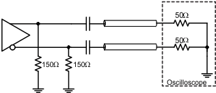
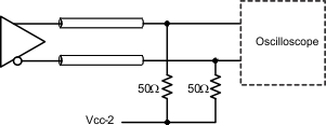
| fclk | Output frequency | Configuration load (see Figure 9 and Figure 10) | 0 | 1175 | MHz | ||
| VOH | LVPECL high-level output voltage | Load | VCC –1.1 | VCC –0.88 | V | ||
| VOL | LVPECL low-level output voltage | Load | VCC –2.02 | VCC –1.48 | V | ||
| |VOD| | Differential output voltage | 510 | 870 | mV | |||
| tsko | Skew, output to output For Y0 to Y1 | Both outputs set at 122.88 MHz | 15 | ps | |||
| CO | Output capacitance on Y0 to Y1 | VCC = 3.3 V; VO = 0 V or VCC | 5 | pF | |||
| IOPDH | Power-down output current | VO = VCC | 25 | μA | |||
| IOPDL | Power-down output current | VO = 0 V | 5 | μA | |||
| Duty cycle | 45% | 55% | |||||
| tr / tf | Rise and fall time | 20% to 80% of VOPP | 55 | 75 | 135 | ps | |
| LVDS-TO- LVPECL | |||||||
| tskP_C | Output skew between LVDS and LVPECL outputs | Crosspoint to Crosspoint | 130 | 200 | 280 | ps | |
| LVCMOS-TO- LVPECL | |||||||
| tskP_C | Output skew between LVCMOS and LVPECL outputs | VCC/2 to Crosspoint | 1.6 | 1.8 | 2.2 | ns | |
| LVPECL Hi-PERFORMANCE OUTPUT | |||||||
| VOH | LVPECL high-level output voltage | Load | VCC –1.11 | VCC –0.91 | V | ||
| VOL | LVPECL low-level output voltage | Load | VCC –2.06 | VCC –1.84 | V | ||
| |VOD| | Differential output voltage | 670 | 950 | mV | |||
| tr / tf | Rise and fall time | 20% to 80% of VOPP | 55 | 75 | 135 | ps | |
7.4 Timing Requirements
over recommended ranges of supply voltage, load and operating free-air temperature range (unless otherwise noted)7.5 SPI Bus Timing Characteristics
| PARAMETER | MIN | TYP | MAX | UNIT | |
|---|---|---|---|---|---|
| fClock | Clock frequency for the SPI_CLK | 20 | MHz | ||
| t1 | SPI_LE to SPI_CLK setup time | 10 | ns | ||
| t2 | SPI_MOSI to SPI_CLK setup time | 10 | ns | ||
| t3 | SPI_MOSI to SPI_CLK hold time | 10 | ns | ||
| t4 | SPI_CLK high duration | 25 | ns | ||
| t5 | SPI_CLK low duration | 25 | ns | ||
| t6 | SPI_CLK to SPI_LE hold time | 10 | ns | ||
| t7 | SPI_LE pulse width | 20 | ns | ||
| t8 | SPI_CLK to MISO data valid | 10 | ns | ||
| t9 | SPI_LE to SPI_MISO data valid | 10 | ns | ||
 Figure 1. Timing Diagram for SPI Write Command
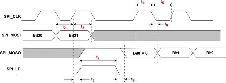 Figure 2. Timing Diagram for SPI Read Command
7.6 Typical Characteristics
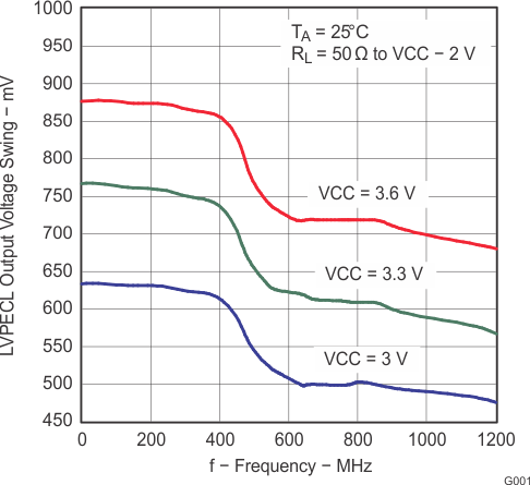 Figure 3. LVPECL Output Voltage Swing vs Frequency
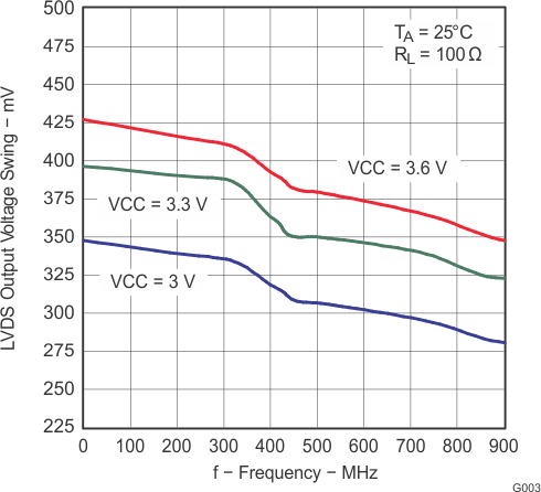 Figure 5. LVDS Output Voltage Swing vs Frequency
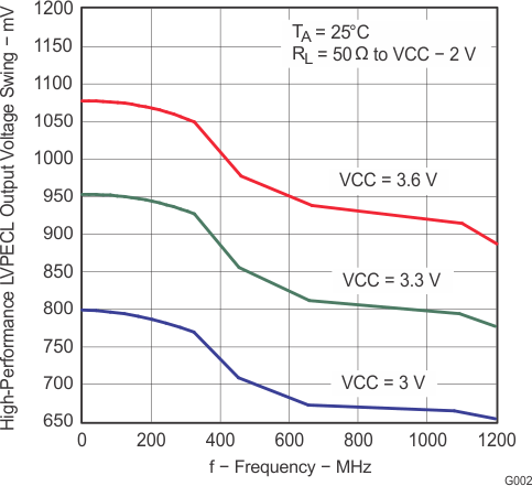 Figure 4. High-Performance LVPECL Output Voltage Swing vs Frequency
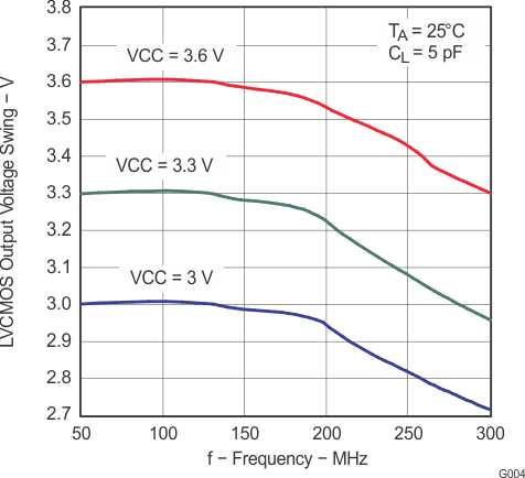 Figure 6. LVCMOS Output Voltage Swing vs Frequency
