SNAS705D January 2017 – February 2024 CDCE813-Q1
PRODUCTION DATA
- 1
- 1 Features
- 2 Applications
- 3 Description
- 4 Pin Configuration and Functions
- 5 Specifications
- 6 Parameter Measurement Information
- 7 Detailed Description
- 8 Application and Implementation
- 9 Register Maps
- 10Device and Documentation Support
- 11Revision History
- 12Mechanical, Packaging, and Orderable Information
Package Options
Mechanical Data (Package|Pins)
- PW|14
Thermal pad, mechanical data (Package|Pins)
Orderable Information
4 Pin Configuration and Functions
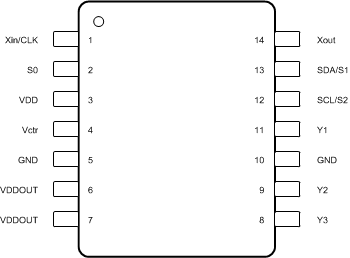
 Figure 4-1 PW Package14-Pin TSSOPTop View
Table 4-1 Pin Functions
| PIN | TYPE(1) | DESCRIPTION | |
|---|---|---|---|
| NAME | NO. | ||
| GND | 5, 10 | G | Ground |
| SCL/S2 | 12 | I | SCL: serial clock input LVCMOS (default configuration), 500-kΩ
internal pullup; or S2: user-programmable control input, LVCMOS input, 500-kΩ internal pullup |
| SDA/S1 | 13 | I/O or I | SDA: bidirectional serial data input or output (default
configuration), LVCMOS internal pullup; or S1: user-programmable control input, LVCMOS input, 500-kΩ internal pullup |
| S0 | 2 | I | User-programmable control input S0, LVCMOS input, 500-kΩ internal
pullup CDCE813-Q1 default: S0 = 1: Y1 is 3-state, S0 = 0: Y1 is 3-state CDCE813R02-Q1 default: S0 = 1: Y1 is enabled, S0 = 0: Y1 is 3-state |
| Vctr | 4 | I | VCXO control voltage (leave open or pull up when not used) |
| VDD | 3 | P | 1.8-V power supply for the device |
| VDDOUT | 6, 7 | P | 3.3-V or 2.5-V supply for all outputs |
| Xin/CLK | 1 | I | Crystal oscillator input or LVCMOS clock input (selectable through the I2C bus) |
| Xout | 14 | O | Crystal oscillator output (leave open or pull up when not used) |
| Y1 | 11 | O | LVCMOS output |
| Y2 | 9 | O | LVCMOS output |
| Y3 | 8 | O | LVCMOS output |
(1) G = Ground, I = Input, O = Output, P = Power