SLAS564H August   2007  – July 2024 CDCE937 , CDCEL937

PRODUCTION DATA  

  1.   1
  2. Features
  3. Applications
  4. Description
  5. Pin Configuration and Functions
  6. Specifications
    1. 5.1 Absolute Maximum Ratings
    2. 5.2 ESD Ratings
    3. 5.3 Recommended Operating Conditions
    4. 5.4 Thermal Information
    5. 5.5 Electrical Characteristics
    6. 5.6 Timing Requirements: CLK_IN
    7. 5.7 Timing Requirements: SDA/SCL
    8. 5.8 EEPROM Specification
    9. 5.9 Typical Characteristics
  7. Parameter Measurement Information
  8. Detailed Description
    1. 7.1 Overview
    2. 7.2 Functional Block Diagram
    3. 7.3 Feature Description
      1. 7.3.1 Control Terminal Setting
      2. 7.3.2 Default Device Setting
      3. 7.3.3 SDA/SCL Serial Interface
      4. 7.3.4 Data Protocol
    4. 7.4 Device Functional Modes
      1. 7.4.1 SDA/SCL Hardware Interface
    5. 7.5 Programming
  9. Register Maps
    1. 8.1 SDA/SCL Configuration Registers
  10. Application and Implementation
    1. 9.1 Application Information
    2. 9.2 Typical Application
      1. 9.2.1 Design Requirements
      2. 9.2.2 Detailed Design Procedure
        1. 9.2.2.1 Spread Spectrum Clock (SSC)
        2. 9.2.2.2 PLL Frequency Planning
        3. 9.2.2.3 Crystal Oscillator Start-Up
        4. 9.2.2.4 Frequency Adjustment With Crystal Oscillator Pulling
        5. 9.2.2.5 Unused Inputs and Outputs
        6. 9.2.2.6 Switching Between XO and VCXO Mode
      3. 9.2.3 Application Curves
  11. 10Power Supply Recommendations
  12. 11Layout
    1. 11.1 Layout Guidelines
    2. 11.2 Layout Example
  13. 12Device and Documentation Support
    1. 12.1 Device Support
      1. 12.1.1 Third-Party Products Disclaimer
      2. 12.1.2 Development Support
    2. 12.2 Documentation Support
      1. 12.2.1 Related Documentation
    3. 12.3 Receiving Notification of Documentation Updates
    4. 12.4 Support Resources
    5. 12.5 Trademarks
    6. 12.6 Electrostatic Discharge Caution
    7. 12.7 Glossary
  14. 13Revision History
  15. 14Mechanical, Packaging, and Orderable Information

Package Options

Mechanical Data (Package|Pins)
Thermal pad, mechanical data (Package|Pins)
Orderable Information

Description

The CDCE937 and CDCEL937 devices are modular PLL-based low cost, high-performance, programmable clock synthesizers, multipliers and dividers. The devices generate up to 7 output clocks from a single input frequency. Each output can be programmed in-system for any clock frequency up to 230MHz, using up to three independent configurable PLLs.

The CDCEx937 has separate output supply pins, VDDOUT, which is 1.8V for CDCEL937 and to 2.5V to 3.3V for CDCE937.

The input accepts an external crystal or LVCMOS clock signal. If an external crystal is used, an on-chip load capacitor is adequate for most applications. The value of the load capacitor is programmable from 0 to 20pF. Additionally, an on-chip VCXO is selectable which allows synchronization of the output frequency to an external control signal, that is, PWM signal.

Device Information
PART NUMBER PACKAGE(1) PACKAGE SIZE(2)
CDCE937, CDCEL937 TSSOP (20) 6.50mm x 6.40mm
For all available packages, see the orderable addendum at the end of the data sheet.
The package size (length × width) is a nominal value and includes pins, where applicable.
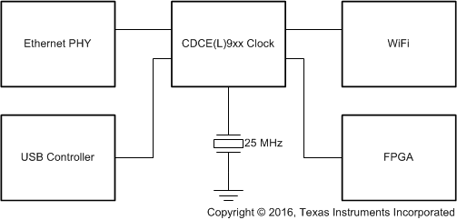
CDCE937 CDCEL937 Typical Application Schematic Typical Application Schematic