SLLSEL1 November 2014 CDCL1810A
PRODUCTION DATA.
- 1 Features
- 2 Applications
- 3 Description
- 4 Simplified Schematic
- 5 Revision History
- 6 Device Comparison Tables
- 7 Pin Configuration and Functions
- 8 Specifications
- 9 Detailed Description
- 10Application and Implementation
- 11Power Supply Recommendations
- 12Layout
- 13Device and Documentation Support
- 14Mechanical, Packaging, and Orderable Information
- 13Mechanical, Packaging, and Orderable Information
Package Options
Mechanical Data (Package|Pins)
- RGZ|48
Thermal pad, mechanical data (Package|Pins)
- RGZ|48
Orderable Information
10 Application and Implementation
NOTE
Information in the following applications sections is not part of the TI component specification, and TI does not warrant its accuracy or completeness. TI’s customers are responsible for determining suitability of components for their purposes. Customers should validate and test their design implementation to confirm system functionality.
10.1 Application Information
The CDCL1810 is a high-performance buffer that can generate 10 copies of CML clock outputs from a LVDS input. The programmable dividers, P0 and P1, give a high flexibility to the ratio of the output frequency to the input frequency.
10.1.1 Clock Distribution for Multiple TI Keystone DSPs
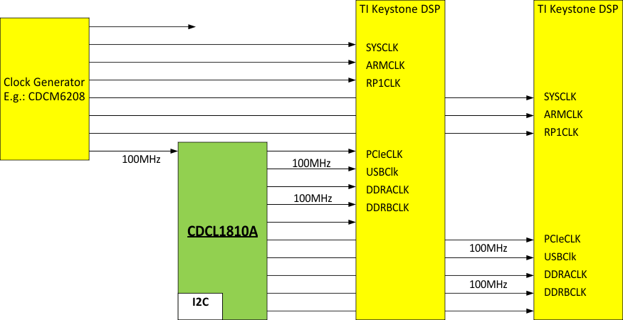 Figure 9. CDCL1810A Application Drawing
10.1.1.1 Design Requirements
A typical application example is multi DSP chip environment. The CDCL1810A is used to buffer the common clocks to the DSP.
10.1.1.2 Detailed Design Procedure
The CDCL1810A does not support output group phase alignment if a divider gets reprogrammed. Both clock groups might be out of phase by multiple input clock cycles. This is especially of concern if both dividers are greater than 1 (see Figure 10).
Continuous operation of output clocks is ensured, while enabling/disabling of outputs in the CDCL1810A. (see Figure 11).
10.1.1.3 Application Curves
 Figure 10. Output Group Divider Change
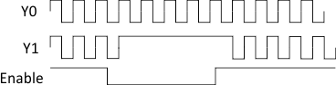 Figure 11. Individual Output Disable/Enable