SCAS895B May 2010 – February 2017 CDCLVC1102 , CDCLVC1103 , CDCLVC1104 , CDCLVC1106 , CDCLVC1108 , CDCLVC1110 , CDCLVC1112
PRODUCTION DATA.
- 1 Features
- 2 Applications
- 3 Description
- 4 Revision History
- 5 Pin Configuration and Functions
- 6 Specifications
- 7 Parameter Measurement Information
- 8 Detailed Description
- 9 Application and Implementation
- 10Power Supply Recommendations
- 11Layout
- 12Device and Documentation Support
- 13Mechanical, Packaging, and Orderable Information
Package Options
Mechanical Data (Package|Pins)
- PW|8
Thermal pad, mechanical data (Package|Pins)
Orderable Information
6 Specifications
6.1 Absolute Maximum Ratings
over operating free-air temperature range (unless otherwise noted) (1)| MIN | MAX | UNIT | ||
|---|---|---|---|---|
| VDD | Supply voltage | –0.5 | 4.6 | V |
| VIN | Input voltage(2) | –0.5 | VDD + 0.5 | V |
| VO | Output voltage(2) | –0.5 | VDD + 0.5 | V |
| IIN | Input current | –20 | 20 | mA |
| IO | Continuous output current | –50 | 50 | mA |
| TJ | Maximum junction temperature | 125 | °C | |
| Tstg | Storage temperature | –65 | 150 | °C |
(1) Stresses beyond those listed under Absolute Maximum Ratings may cause permanent damage to the device. These are stress ratings only and functional operation of the device at these or any other conditions beyond those indicated under Recommended Operating Conditions is not implied. Exposure to absolute-maximum-rated conditions for extended periods may affect device reliability.
(2) This value is limited to 4.6 V maximum.
6.2 ESD Ratings
| VALUE | UNIT | |||
|---|---|---|---|---|
| V(ESD) | Electrostatic discharge | Human-body model (HBM), per ANSI/ESDA/JEDEC JS-001(1) | ±4000 | V |
| Charged-device model (CDM), per JEDEC specification JESD22-C101(2) | ±1500 | |||
(1) JEDEC document JEP155 states that 500-V HBM allows safe manufacturing with a standard ESD control process.
(2) JEDEC document JEP157 states that 250-V CDM allows safe manufacturing with a standard ESD control process.
6.3 Recommended Operating Conditions
over operating free-air temperature range (unless otherwise noted)| MIN | NOM | MAX | UNIT | |||
|---|---|---|---|---|---|---|
| VDD | Supply voltage | 3.3-V supply | 3.0 | 3.3 | 3.6 | V |
| 2.5-V supply | 2.3 | 2.5 | 2.7 | |||
| VIL | Low-level input voltage | VDD = 3.0 V to 3.6 V | VDD/2 – 600 | mV | ||
| VDD = 2.3 V to 2.7 V | VDD/2 – 400 | |||||
| VIH | High-level input voltage | VDD = 3.0 V to 3.6 V | VDD/2 + 600 | mV | ||
| VDD = 2.3 V to 2.7 V | VDD/2 + 400 | |||||
| Vth | Input threshold voltage | VDD = 2.3 V to 3.6 V | VDD/2 | mV | ||
| tr / tf | Input slew rate | 1 | 4 | V/ns | ||
| tw | Minimum pulse width at CLKIN | VDD = 3.0 V to 3.6 V | 1.8 | ns | ||
| VDD = 2.3 V to 2.7 V | 2.75 | |||||
| fCLK | LVCMOS clock Input Frequency | VDD = 3.0 V to 3.6 V | DC | 250 | MHz | |
| VDD = 2.3 V to 2.7 V | DC | 180 | ||||
| TA | Operating free-air temperature | –40 | 85 | °C | ||
6.4 Thermal Information
| THERMAL METRIC(1) | CDCLVC1102 CDCLVC1103 CDCLVC1104 |
CDCLVC1106 | CDCLVC1108 | CDCLVC11010 | CDCLVC1112 | UNIT | |
|---|---|---|---|---|---|---|---|
| PW (TSSOP) | |||||||
| 8 PINS | 14 PINS | 16 PINS | 20 PINS | 24 PINS | |||
| RθJA | Junction-to-ambient thermal resistance(2) | 149.4 | 112.6 | 108.4 | 83.0 | 87.9 | °C/W |
| RθJC(top) | Junction-to-case(top) thermal resistance (3) | 69.4 | 48.0 | 33.6 | 32.3 | 26.5 | °C/W |
(1) For more information about traditional and new thermal metrics, see the IC Package Thermal Metrics application report.
(2) The junction-to-ambient thermal resistance under natural convection is obtained in a simulation on a JEDEC-standard, high-K board, as specified in JESD51-7, in an environment described in JESD51-2a.
(3) The junction-to-case (top) thermal resistance is obtained by simulating a cold plate test on the package top. No specific JEDEC-standard test exists, but a close description can be found in the ANSI SEMI standard G30-88.
6.5 Electrical Characteristics
Over recommended operating free-air temperature range (unless otherwise noted)| PARAMETER | TEST CONDITIONS | MIN | TYP(1) | MAX | UNIT | |
|---|---|---|---|---|---|---|
| OVERALL PARAMETERS FOR ALL VERSIONS | ||||||
| IDD | Static device current(2) | 1G = VDD; CLKIN = 0 V or VDD; IO = 0 mA; VDD = 3.6 V | 6 | 10 | mA | |
| 1G = VDD; CLKIN = 0 V or VDD; IO = 0 mA; VDD = 2.7 V | 3 | 6 | ||||
| IPD | Power-down current | 1G = 0 V; CLKIN = 0 V or VDD; IO = 0 mA; VDD = 3.6 V or 2.7 V | 60 | µA | ||
| CPD | Power dissipation capacitance per output(3) | VDD = 3.3 V; f = 10 MHz | 6 | pF | ||
| VDD = 2.5 V; f = 10 MHz | 4.5 | |||||
| II | Input leakage current at 1G | VI = 0 V or VDD, VDD = 3.6 V or 2.7 V | 8 | 8 | µA | |
| Input leakage current at CLKIN | 25 | 25 | ||||
| ROUT | Output impedance | VDD = 3.3 V | 45 | Ω | ||
| VDD = 2.5 V | 60 | |||||
| fOUT | Output frequency | VDD = 3 V to 3.6 V | DC | 250 | MHz | |
| VDD = 2.3 V to 2.7 V | DC | 180 | ||||
| OUTPUT PARAMETERS FOR VDD = 3.3 V ± 0.3 V | ||||||
| VOH | High-level output voltage | VDD = 3 V, IOH = –0.1 mA | 2.9 | V | ||
| VDD = 3 V, IOH = –8 mA | 2.5 | |||||
| VDD = 3 V, IOH = –12 mA | 2.2 | |||||
| VOL | Low-level output voltage | VDD = 3 V, IOL = 0.1 mA | 0.1 | V | ||
| VDD = 3 V, IOL = 8 mA | 0.5 | |||||
| VDD = 3 V, IOL = 12 mA | 0.8 | |||||
| OUTPUT PARAMETERS FOR VDD = 2.5 V ± 0.2 V | ||||||
| VOH | High-level output voltage | VDD = 2.3 V, IOH = –0.1 mA | 2.2 | V | ||
| VDD = 2.3 V, IOH = –8 mA | 1.7 | |||||
| VOL | Low-level output voltage | VDD = 2.3 V, IOL = 0.1 mA | 0.1 | V | ||
| VDD = 2.3 V, IOL = 8 mA | 0.5 | |||||
(1) All typical values are at respective nominal VDD. For switching characteristics, outputs are terminated to 50 Ω to VDD/2 (see Figure 3).
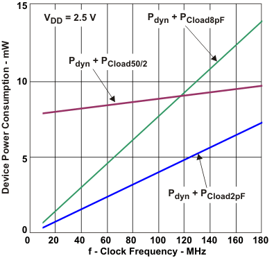
(2) For dynamic IDD over frequency see and Figure 1.
(3) This is the formula for the power dissipation calculation (see and the Power Considerations section).
Ptot = Pstat + Pdyn + PCload [W]
Pstat = VDD × IDD [W]
Pdyn = CPD × VDD2 × ƒ [W]
PCload = Cload × VDD2 × ƒ × n [W]
n = Number of switching output pins
Ptot = Pstat + Pdyn + PCload [W]
Pstat = VDD × IDD [W]
Pdyn = CPD × VDD2 × ƒ [W]
PCload = Cload × VDD2 × ƒ × n [W]
n = Number of switching output pins
(4) tsk(p) depends on output rise- and fall-time (tr/tf). The output duty-cycle can be calculated: odc = (tw(OUT) ± tsk(p))/tperiod; tw(OUT) is pulse-width of output waveform and tperiod is 1/fOUT.
(5) Parameter is specified by characterization. Not tested in production.
6.6 Switching Characteristics
over operating free-air temperature range (unless otherwise noted)| PARAMETER | TEST CONDITIONS | MIN | TYP | MAX | UNIT | |
|---|---|---|---|---|---|---|
| OUTPUT PARAMETERS FOR VDD = 3.3 V ± 0.3 V | ||||||
| tPLH, tPHL | Propagation delay | CLKIN to Yn | 0.8 | 2.0 | ns | |
| tsk(o) | Output skew | Equal load of each output | 50 | ps | ||
| tr/tf | Rise and fall time | 20%–80% (VOH - VOL) | 0.3 | 0.8 | ns | |
| tDIS | Output disable time | 1G to Yn | 6 | ns | ||
| tEN | Output enable time | 1G to Yn | 6 | ns | ||
| tsk(p) | Pulse skew ; tPLH(Yn) – tPHL(Yn) (4) |
To be measured with input duty cycle of 50% | 180 | ps | ||
| tsk(pp) | Part-to-part skew | Under equal operating conditions for two parts | 0.5 | ns | ||
| tjitter | Additive jitter rms(5) | 12 kHz to 20 MHz, fOUT = 250 MHz | 100 | fs | ||
| OUTPUT PARAMETERS FOR VDD = 2.5 V ± 0.2 V | ||||||
| tPLH, tPHL | Propagation delay | CLKIN to Yn | 1 | 2.6 | ns | |
| tsk(o) | Output skew | Equal load of each output | 50 | ps | ||
| tr/tf | Rise and fall time | 20%–80% reference point | 0.3 | 1.2 | ns | |
| tDIS | Output disable time | 1G to Yn | 10 | ns | ||
| tEN | Output enable time | 1G to Yn | 10 | ns | ||
| tsk(p) | Pulse skew ; tPLH(Yn) – tPHL(Yn) (4) |
To be measured with input duty cycle of 50% | 220 | ps | ||
| tsk(pp) | Part-to-part skew | Under equal operating conditions for two parts | 1.2 | ns | ||
| tjitter | Additive jitter rms(5) | 12 kHz to 20 MHz, fOUT = 180 MHz | 350 | fs | ||
6.7 Typical Characteristics
 Figure 1. Device Power Consumption vs Clock Frequency
(Load 50 Ω into VDD/2; 2 pF, 8 pF; Per Output)
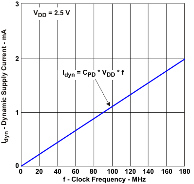
 Figure 2. Dynamic Supply Current vs Clock Frequency
 (CPD = 4.5 pF, No Load; Per Output)