SCAS841D February 2007 – December 2016 CDCLVD110A
PRODUCTION DATA.
- 1 Features
- 2 Applications
- 3 Description
- 4 Revision History
- 5 Pin Configuration and Functions
- 6 Specifications
- 7 Parameter Measurement Information
- 8 Detailed Description
- 9 Application and Implementation
- 10Power Supply Recommendations
- 11Layout
- 12Device and Documentation Support
- 13Mechanical, Packaging, and Orderable Information
Package Options
Mechanical Data (Package|Pins)
Thermal pad, mechanical data (Package|Pins)
- RHB|32
Orderable Information
1 Features
- Low-Output Skew <30 ps (Typical) for Clock-Distribution Applications
- Distributes One Differential Clock Input to
10 LVDS Differential Clock Outputs - VCC Range: 2.5 V ±5%
- Typical Signaling Rate Capability of Up to
1.1 GHz - Configurable Register (SI/CK) Individually Enables Disables Outputs, Selectable CLK0, CLK0 or CLK1, CLK1 Inputs
- Full Rail-to-Rail Common-Mode Input Range
- Receiver Input Threshold: ±100 mV
- Available in 32-Pin LQFP and VQFN Package
- Fail-Safe I/O-Pins for VDD = 0 V (Power Down)
3 Description
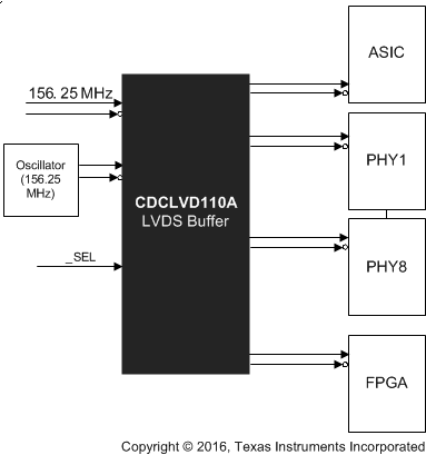
The CDCLVD110A clock driver distributes one pair of differential LVDS clock inputs (either CLK0 or CLK1) to 10 pairs of differential clock outputs (Q0 to Q9) with minimum skew for clock distribution. The CDCLVD110A is specifically designed to drive 50-Ω transmission lines.
When the control enable is high (EN = 1), the 10 differential outputs are programmable in that each output can be individually enabled or disabled
(3-stated) according to the first 10 bits loaded into the shift register. Once the shift register is loaded, the last bit selects either CLK0 or CLK1 as the clock input. However, when EN = 0, the outputs are not programmable and all outputs are enabled.
The CDCLVD110A has an improved start-up circuit that minimizes enabling time in AC- and DC-coupled systems.
The CDCLVD110A is characterized for operation from –40°C to 85°C.
Device Information(1)
| PART NUMBER | PACKAGE | BODY SIZE (NOM) |
|---|---|---|
| CDCLVD110A | LQFN (32) | 7.00 mm × 7.00 mm |
| VQFN (32) | 5.00 mm × 5.00 mm |
- For all available packages, see the orderable addendum at the end of the data sheet.
Application Example
