SCAS841D February 2007 – December 2016 CDCLVD110A
PRODUCTION DATA.
- 1 Features
- 2 Applications
- 3 Description
- 4 Revision History
- 5 Pin Configuration and Functions
- 6 Specifications
- 7 Parameter Measurement Information
- 8 Detailed Description
- 9 Application and Implementation
- 10Power Supply Recommendations
- 11Layout
- 12Device and Documentation Support
- 13Mechanical, Packaging, and Orderable Information
Package Options
Mechanical Data (Package|Pins)
Thermal pad, mechanical data (Package|Pins)
- RHB|32
Orderable Information
11 Layout
11.1 Layout Guidelines
Power consumption of the CDCLVP111 can be high enough to require attention to thermal management. For reliability and performance reasons, the die temperature must be limited to a maximum of 110°C. That is, as an estimate, ambient temperature (TA) plus device power consumption times RθJA must not exceed 110°C.
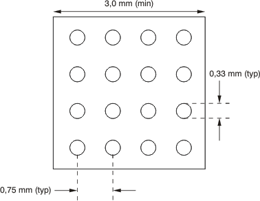
The device package has an exposed pad that provides the primary heat removal path to the printed-circuit board (PCB). To maximize the heat dissipation from the package, a thermal landing pattern including multiple vias to a ground plane must be incorporated into the PCB within the footprint of the package. The exposed pad must be soldered down to ensure adequate heat conduction out of the package. Figure 18 shows a recommended land and via pattern.
11.2 Layout Example
 Figure 18. Recommended PCB Layout
11.3 Thermal Considerations
The CDCLVD110A supports high temperatures on the printed-circuit board (PCB) measured at the thermal pad. The system designer must ensure that the maximum junction temperature is not exceeded. ΨJB can allow the system designer to measure the board temperature with a fine gauge thermocouple and back calculate the junction temperature using Equation 1. Note that ΨJB is close to RθJB as 75% to 95% of a device's heat is dissipated by the PCB.
| Example: | ||
| Calculation of the junction-lead temperature with a 4-layer JEDEC test board using four thermal vias: | ||
| TPCB = 85°C | ||
| ΨJB = 17.9°C/W | ||
| PowerinclTerm = Imax × Vmax = 160 mA × 3.6 V = 576 mW (maximum power consumption including termination resistors) | ||
| PowerexclTerm = 550.8 mW (maximum power consumption excluding termination resistors, see Power Consumption of LVPECL and LVDS for further details) | ||
| ΔTJ = ΨJB × PowerexclTerm = 9.86°C/W × 550.8 mW = 9.86°C | ||
| TJ = ΔTJ + TChassis = 17.9°C + 85°C = 95.86°C (maximum junction temperature of 125°C is not violated) | ||
Further information can be found at Semiconductor and IC Package Thermal Metrics (SPRA953) and Using Thermal Calculation Tools for Analog Components (SLUA566).