SCAS759C April 2004 – July 2017 CDCM1802
PRODUCTION DATA.
- 1 Features
- 2 Applications
- 3 Description
- 4 Revision History
- 5 Pin Configuration and Functions
-
6 Specifications
- 6.1 Absolute Maximum Ratings
- 6.2 ESD Ratings
- 6.3 Recommended Operating Conditions
- 6.4 Thermal Information
- 6.5 Electrical Characteristics
- 6.6 Switching Characteristics
- 6.7 Jitter Characteristics
- 6.8 Supply Current Electrical Characteristics
- 6.9 Control Input Characteristics
- 6.10 Timing Requirements
- 6.11 Bias Voltage VBB
- 6.12 Typical Characteristics
- 7 Parameter Measurement Information
- 8 Detailed Description
- 9 Application and Implementation
- 10Power Supply Recommendations
- 11Layout
- 12Device and Documentation Support
- 13Mechanical, Packaging, and Orderable Information
Package Options
Mechanical Data (Package|Pins)
- RGT|16
Thermal pad, mechanical data (Package|Pins)
- RGT|16
Orderable Information
8 Detailed Description
8.1 Overview
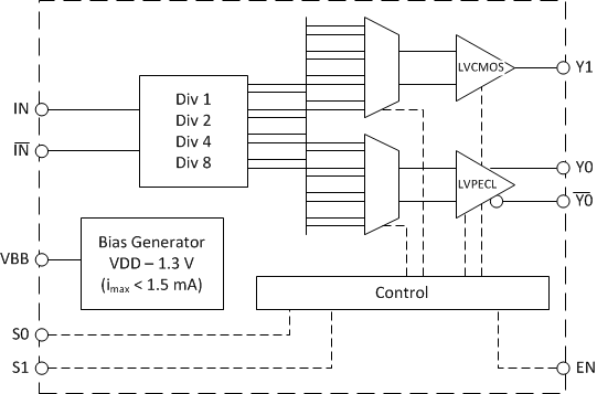
The CDCM1802 is a clock buffer with a programmable divider. There is one LVCMOS and one LVPECL output. The LVCMOS output is specifically designed for driving 50-Ω transmission lines. It is delayed by 1.6 ns over the PECL output stage to minimize noise impact during signal transitions. Both outputs can be divided individually by 1, 2, 4, and 8. Divider settings can be selected with three 3-level control pins.
8.2 Functional Block Diagram
8.3 Feature Description
The CDCM1802 has two control pins, S0 and S1, to select different output mode settings. The S[1:0] pins are 3-level inputs. Additionally, an enable pin EN is provided to disable or enable all outputs simultaneously. For single-ended driver applications, the CDCM1802 provides a VBB output pin that can be directly connected to the unused input as a common-mode voltage reference.
8.4 Device Functional Modes
8.4.1 Control Pin Settings
The CDCM1802 has three control pins, S0, S1, and the enable pin (EN) to select different output mode settings. All three inputs (S0, S1, EN) are 3-level inputs. In addition, the EN input allows disabling all outputs and place them into a Hi-Z (or tristate) output state when pulled to GND.
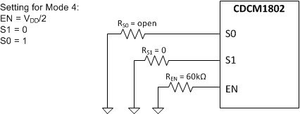 Figure 11. Control Pin Setting for Example
Each control input incorporates a 60-kΩ pullup resistor. Thus, it is easy to choose the input setting by designing a resistor pad between the control input and GND. To choose a logic zero, the resistor value must be zero. Setting the input high requires leaving the resistor pad empty (no resistor installed). For setting the input to VDD/2, the installed resistor needs a value of 60 kΩ with a tolerance better or equal to 10%.
Table 1. Selection Mode Table
| MODE | EN | S1 | S0 | LVPECL(1) | LVCMOS |
|---|---|---|---|---|---|
| Y0 | Y1 | ||||
| 0 | 0 | X | X | Off (high-z) | Off (high-z) |
| 1 | VDD/2 | 0 | VDD/2 | /1 | /1 |
| 2 | VDD/2 | VDD/2 | 1 | /1 | /2 |
| 3 | 1 | 0 | 0 | /1 | /4 |
| 4 | VDD/2 | 0 | 1 | /2 | /2 |
| 5 | 1 | 0 | 1 | /2 | /4 |
| 6 | VDD/2 | 0 | 0 | /4 | /4 |
| 7 | VDD/2 | 1 | 0 | /4 | /8 |
| 8 | VDD/2 | VDD/2 | VDD/2 | /8 | /1 |
| 9 | 1 | 1 | 0 | /8 | /4 |
| 10 | 1 | 1 | 1 | Off (high-z) | /4 |
8.4.2 Device Behavior During RESET and Control Pin Switching
8.4.2.1 Output Behavior When Enabling the Device (EN = 0 → 1)
In disable mode (EN = 0), all output drivers are switched in high-Z mode. The bandgap, current references, the amplifier, and the S0 and S1 control inputs are also switched off. In the same mode, all flip-flops will be reset. The typical current consumption is likely below 500 µA (to be measured).
When the device will be enabled again it takes maximal 1 µs for the settling of the reference voltage and currents. During this time the output Y0 and Y0 drive a high signal. Y1 is unknown (could be high or low). After the settle time, the outputs go into the low state. Due to the synchronization of each output driver signal with the input clock, the state of the waveforms after enabling the device look like those shown in Figure 12. The inverting input and output signal is not included. The Y:/1 waveform is the undivided output driver state.
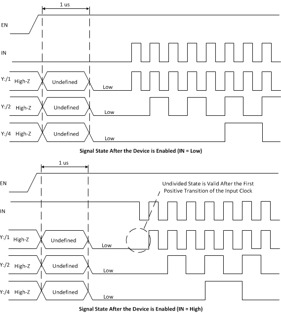 Figure 12. Waveforms
8.4.2.2 Enabling a Single Output Stage
If a single output stage becomes enabled:
- Y0 will either be low or high (undefined).
- Y0 will be the inverted signal of Y0.
With the first positive clock transition, the undivided output becomes the input clock state. If a divide mode is used, the divided output states are equal to the actual internal divider. The internal divider does not get a reset while enabling single output drivers.
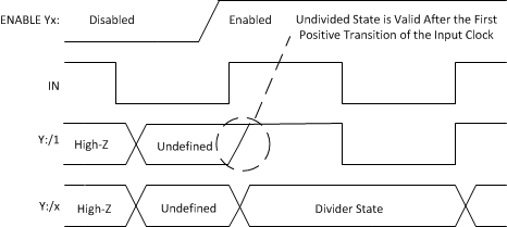 Figure 13. Signal State After an Output Driver Becomes Enabled While IN = 0
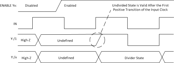 Figure 14. Signal State After an Output Driver Becomes Enabled While IN = 1