SCAS759C April 2004 – July 2017 CDCM1802
PRODUCTION DATA.
- 1 Features
- 2 Applications
- 3 Description
- 4 Revision History
- 5 Pin Configuration and Functions
-
6 Specifications
- 6.1 Absolute Maximum Ratings
- 6.2 ESD Ratings
- 6.3 Recommended Operating Conditions
- 6.4 Thermal Information
- 6.5 Electrical Characteristics
- 6.6 Switching Characteristics
- 6.7 Jitter Characteristics
- 6.8 Supply Current Electrical Characteristics
- 6.9 Control Input Characteristics
- 6.10 Timing Requirements
- 6.11 Bias Voltage VBB
- 6.12 Typical Characteristics
- 7 Parameter Measurement Information
- 8 Detailed Description
- 9 Application and Implementation
- 10Power Supply Recommendations
- 11Layout
- 12Device and Documentation Support
- 13Mechanical, Packaging, and Orderable Information
Package Options
Mechanical Data (Package|Pins)
- RGT|16
Thermal pad, mechanical data (Package|Pins)
- RGT|16
Orderable Information
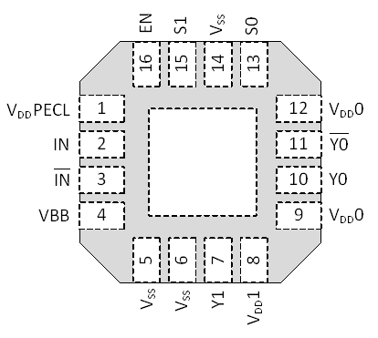
5 Pin Configuration and Functions
RGT Package
16-Pin VQFN
Top View

Pin Functions
| PIN | I/O | DESCRIPTION | |
|---|---|---|---|
| NAME | NO. | ||
| EN | 16 | I (with 60-kΩ pullup) |
ENABLE. Enables or disables all outputs simultaneously; The EN pin offers three different configurations: tie to GND (logic 0), external 60-kΩ pulldown resistor (pull to VDD/2) or left floating (logic 1); EN = 1: outputs on according to S0 and S1 setting EN = VDD/2: outputs on according to S0 and S1 setting EN = 0; outputs Y[1:0] off (high-impedance); see Table 1 for details. |
| IN | 2 | I Differential input |
Differential input clock. Input stage is sensitive and has a wide common mode range. Therefore, almost any type of differential signal can drive this input (LVPECL, LVDS, CML, HSTL). Since the input is high-impedance, it is recommended to terminate the PCB transmission line before the input (for example, with 100-Ω across input). The input can also be driven by a single-ended signal, if the complementary input is tied to a dc reference voltage (for example, VCC/2). The inputs deploy an ESD structure protecting the inputs in case of an input voltage exceeding the rails by more than ≈0.7 V. Reverse biasing of the IC through this inputs is possible and must be prevented by limiting the input voltage < VDD. |
| IN | 3 | ||
| S0 | 13 | I | Select mode of operation. Defines the output configuration of Y0 and Y1. Each pin offers three different configurations: tied to GND (logic 0), external 60-kΩ pulldown resistor (pull to VDD/2) or left floating (logic 1); see Table 1 for details. |
| S1 | 15 | I (with 60-kΩ pullup) |
|
| Y1 | 7 | O | LVCMOS clock output. This output provides a copy of IN or a divided down copy of clock IN based on the selected mode of operation: S0, S1, and EN. Also, this output can be disabled by tying VDD1 to GND. |
| Y0 | 10 | O LVPECL |
LVPECL clock output. This output provides a copy of IN or a divided down copy of clock IN based on the selected mode of operation: S1, S0, and EN. If Y0 output is unused, the output can simply be left open to save power and minimize noise impact to Y1. |
| Y0 | 11 | ||
| VBB | 4 | O | Output bias voltage used to bias unused complementary input IN for single-ended input signals. The output voltage of VBB is VDD −1.3 V. When driving a load, the output current drive is limited to about 1.5 mA. |
| VDDPECL(1) | 1 | Supply | Supply voltage PECL input + internal logic |
| VDD0(1) | 9, 12 | Supply | PECL output supply voltage for output Y0; Y0 can be disabled by pulling VDD0 to GND. Caution: In this mode no voltage from outside may be forced because internal diodes could be forced in a forward direction. Thus, it is recommended to leave the output disconnected. |
| VDD1 | 8 | Supply | Supply voltage CMOS output; The CMOS output can be disabled by pulling VDD1 to GND. Caution: In this mode no voltage from outside may be forced, because internal diodes could be forced in forward direction. Thus, it is recommended to leave Y1 unconnected, tied to GND, or terminated into GND. |
| VSS | 5, 6, 14 | Supply | Device ground |
(1) VDD0, VDD1, and VDDPECL should have the same value.