SCAS643I September 2000 – October 2017 CDCV304
PRODUCTION DATA.
- 1Features
- 2Description
- 3Revision History
- 4Pin Configuration and Functions
- 5Specifications
- 6Parameter Measurement Information
- 7Detailed Description
- 8Device and Documentation Support
- 9Mechanical, Packaging, and Orderable Information
Package Options
Mechanical Data (Package|Pins)
- PW|8
Thermal pad, mechanical data (Package|Pins)
Orderable Information
7 Detailed Description
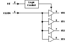
7.1 Functional Block Diagram

7.2 Device Functional Modes
Table 1. Function Table
| INPUTS | OUTPUTS | |
|---|---|---|
| CLKIN | OE | 1Y[0:3] |
| L | L | L |
| H | L | L |
| L | H | L |
| H | H | H |