SCAS666D June 2001 – October 2015 CDCVF2310
PRODUCTION DATA.
- 1 Features
- 2 Applications
- 3 Description
- 4 Revision History
- 5 Pin Configuration and Functions
- 6 Specifications
- 7 Parameter Measurement Information
- 8 Detailed Description
- 9 Application and Implementation
- 10Power Supply Recommendations
- 11Layout
- 12Device and Documentation Support
- 13Mechanical, Packaging, and Orderable Information
Package Options
Refer to the PDF data sheet for device specific package drawings
Mechanical Data (Package|Pins)
- PW|24
Thermal pad, mechanical data (Package|Pins)
Orderable Information
11 Layout
11.1 Layout Guidelines
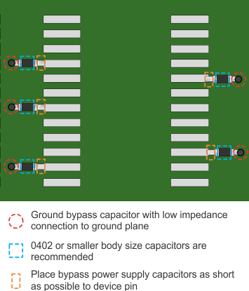
Figure 12 shows a conceptual layout detailing recommended placement of power supply bypass capacitors. For component side mounting, use 0402 body size capacitors to facilitate signal routing. Keep the connections between the bypass capacitors and the power supply on the device as short as possible. Ground the other side of the capacitor using a low-impedance connection to the ground plane.
11.2 Layout Example
 Figure 12. PCB Conceptual Layout
11.3 Thermal Considerations
CDCVF2310 supports high ambient temperature up to 105°C. The system designer needs to ensure that the maximum junction temperature is not exceeded. Following Equation 1 can be used to calculate the junction temperature based on the measured case temperature. The case temperature is defined as the hottest temperature on the top of the device. The case temperature measurement can be performed with (in order of accuracy) an IR camera, a fluor-optic probe, a thermocouple, or IR gun with a maximum field view of 4-mm diameter just to name a few techniques. Further information can be found at SPRA953 and SLUA566