SCAS637E April 2004 – February 2024 CDCVF2509
PRODUCTION DATA
- 1
- 1Features
- 2Applications
- 3Description
- Pin Configuration and Functions
- 4Specifications
- 5Parameter Measurement Information
- 6Device and Documentation Support
- 7Revision History
- 8Mechanical, Packaging, and Orderable Information
Package Options
Refer to the PDF data sheet for device specific package drawings
Mechanical Data (Package|Pins)
- PW|24
Thermal pad, mechanical data (Package|Pins)
Orderable Information
Pin Configuration and Functions
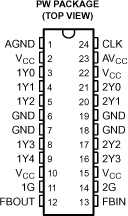
Table 4-1 Pin Functions
| PIN | TYPE | DESCRIPTION | |
|---|---|---|---|
| NAME | NO. | ||
| CLK | 24 | I | Clock input. CLK provides the clock signal to be distributed by the CDCVF2509A clock driver. CLK is used to provide the reference signal to the integrated PLL that generates the clock output signals. CLK must have a fixed frequency and fixed phase for the PLL to obtain phase lock. Once the circuit is powered up and a valid CLK signal is applied, a stabilization time is required for the PLL to phase lock the feedback signal to its reference signal. |
| FBIN | 13 | I | Feedback input. FBIN provides the feedback signal to the internal PLL. FBIN must be hard-wired to FBOUT to complete the PLL. The integrated PLL synchronizes CLK and FBIN so that there is nominally zero phase error between CLK and FBIN. |
| 1G | 11 | I | Output bank enable. 1G is the output enable for outputs 1Y(0:4). When 1G is low, outputs 1Y(0:4) are disabled to a logic-low state. When 1G is high, all outputs 1Y(0:4) are enabled and switch at the same frequency as CLK. |
| 2G | 14 | I | Output bank enable. 2G is the output enable for outputs 2Y(0:3). When 2G is low, outputs 2Y(0:3) are disabled to a logic low state. When 2G is high, all outputs 2Y(0:3) are enabled and switch at the same frequency as CLK. |
| FBOUT | 12 | O | Feedback output. FBOUT is dedicated for external feedback. It switches at the same frequency as CLK. When externally wired to FBIN, FBOUT completes the feedback loop of the PLL. FBOUT has an integrated 25-Ω series-damping resistor. |
| 1Y (0:4) | 3, 4, 5, 8, 9 | O | Clock outputs. These outputs provide low-skew copies of CLK. Output bank 1Y(0:4) is enabled via the 1G input. These outputs can be disabled to a logic-low state by deasserting the 1G control input. Each output has an integrated 25-Ω series-damping resistor. |
| 2Y (0:3) | 16, 17, 21, 20 | O | Clock outputs. These outputs provide low-skew copies of CLK. Output bank 2Y(0:3) is enabled via the 2G input. These outputs can be disabled to a logic-low state by deasserting the 2G control input. Each output has an integrated 25-Ω series-damping resistor. |
| AVCC | 23 | Power | Analog power supply. AVCC provides the power reference for the analog circuitry. In addition, AVCC can be used to bypass the PLL. When AVCC is strapped to ground, PLL is bypassed and CLK is buffered directly to the device outputs. |
| AGND | 1 | Ground | Analog ground. AGND provides the ground reference for the analog circuitry. |
| VCC | 2, 10, 15, 22 | Power | Power supply |
| GND | 6, 7, 18, 19 | Ground | Ground |