SLPS432C November   2012  – January 2015 CSD16556Q5B

PRODUCTION DATA.  

  1. 1Features
  2. 2Applications
  3. 3Description
  4. 4Revision History
  5. 5Specifications
    1. 5.1 Electrical Characteristics
    2. 5.2 Thermal Information
    3. 5.3 Typical MOSFET Characteristics
  6. 6Device and Documentation Support
    1. 6.1 Trademarks
    2. 6.2 Electrostatic Discharge Caution
    3. 6.3 Glossary
  7. 7Mechanical, Packaging, and Orderable Information
    1. 7.1 Q5B Package Dimensions
    2. 7.2 Recommended PCB Pattern
    3. 7.3 Recommended Stencil Pattern
    4. 7.4 Q5B Tape and Reel Information

Package Options

Refer to the PDF data sheet for device specific package drawings

Mechanical Data (Package|Pins)
  • DNK|8
Thermal pad, mechanical data (Package|Pins)
Orderable Information

5 Specifications

5.1 Electrical Characteristics

(TA = 25°C unless otherwise stated)
PARAMETER TEST CONDITIONS MIN TYP MAX UNIT
STATIC CHARACTERISTICS
BVDSS Drain-to-Source Voltage VGS = 0 V, IDS = 250 μA 25 V
IDSS Drain-to-Source Leakage Current VGS = 0 V, VDS = 24 V 1 μA
IGSS Gate-to-Source Leakage Current VDS = 0 V, VGS = 20 V 100 nA
VGS(th) Gate-to-Source Threshold Voltage VDS = VGS, IDS = 250 μA 1.2 1.4 1.7 V
RDS(on) Drain-to-Source On-Resistance VGS = 4.5 V, IDS = 30 A 1.2 1.5
VGS = 10 V, IDS = 30 A 0.9 1.07
gƒs Transconductance VDS = 15 V, IDS = 30 A 191 S
DYNAMIC CHARACTERISTICS
Ciss Input Capacitance VGS = 0 V, VDS = 15 V,
ƒ = 1MHz
4750 6180 pF
Coss Output Capacitance 2270 2950 pF
Crss Reverse Transfer Capacitance 220 280 pF
RG Series Gate Resistance 0.7 1.4 Ω
Qg Gate Charge Total (4.5 V) VDS = 15 V, IDS = 30 A 36 47 nC
Qgd Gate Charge Gate-to-Drain 12 nC
Qgs Gate Charge Gate-to-Source 11 nC
Qg(th) Gate Charge at Vth 7 nC
Qoss Output Charge VDS = 15 V, VGS = 0 V 45 nC
td(on) Turn On Delay Time VDS = 15 V, VGS = 4.5 V,
IDS = 30 A,RG = 2 Ω
17 ns
tr Rise Time 34 ns
td(off) Turn Off Delay Time 25 ns
tƒ Fall Time 13 ns
DIODE CHARACTERISTICS
VSD Diode Forward Voltage ISD = 30 A, VGS = 0 V 0.8 1 V
Qrr Reverse Recovery Charge VDD= 15 V, IF = 30 A, di/dt = 300 A/μs 84 nC
trr Reverse Recovery Time 41 ns

5.2 Thermal Information

(TA = 25°C unless otherwise stated)
THERMAL METRIC MIN TYP MAX UNIT
RθJC Junction-to-Case Thermal Resistance(1) 1.3 °C/W
RθJA Junction-to-Ambient Thermal Resistance(1)(2) 50
(1) RθJC is determined with the device mounted on a 1-inch2 (6.45-cm2), 2-oz. (0.071-mm thick) Cu pad on a 1.5-inches × 1.5-inches
(3.81-cm × 3.81-cm), 0.06-inch (1.52-mm) thick FR4 PCB. RθJC is specified by design, whereas RθJA is determined by the user’s board design.
(2) Device mounted on FR4 material with 1-inch2 (6.45-cm2), 2-oz. (0.071-mm thick) Cu.
M0137-01_LPS198.gif
Max RθJA = 50°C/W when mounted on 1 inch2 (6.45 cm2) of
2-oz. (0.071-mm thick) Cu.
M0137-02_LPS198.gif
Max RθJA = 125°C/W when mounted on a minimum pad area of 2-oz.
(0.071-mm thick) Cu.

5.3 Typical MOSFET Characteristics

(TA = 25°C unless otherwise stated)
graph01_SLPS392B.png
Figure 1. Transient Thermal Impedance
graph02_SLPS431.png
Figure 2. Saturation Characteristics
graph04_SLPS431.png
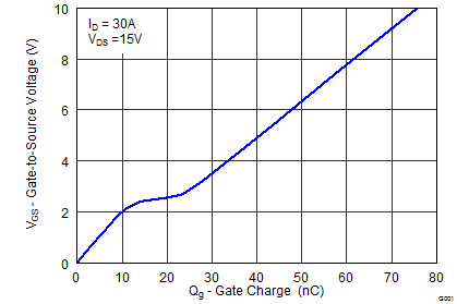
Figure 4. Gate Charge
graph06_SLPS431.png
Figure 6. Threshold Voltage vs Temperature
graph08_SLPS431.png
Figure 8. Normalized On-State Resistance vs Temperature
graph10_SLPS432C.png
Figure 10. Maximum Safe Operating Area (SOA)
graph12_SLPS431.png
Figure 12. Maximum Drain Current vs Temperature
graph03_SLPS431.png
Figure 3. Transfer Characteristics
graph05_SLPS431.png
Figure 5. Capacitance
graph07_SLPS431.png
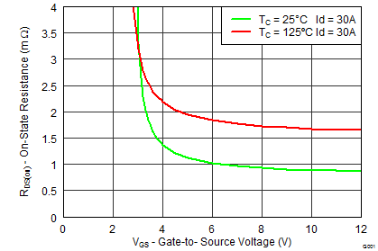
Figure 7. On-State Resistance vs Gate-to-Source Voltage
graph09_SLPS431.png
Figure 9. Typical Diode Forward Voltage
graph11_SLPS431.png
Figure 11. Single Pulse Unclamped Inductive Switching