SLPS262C February 2010 – December 2019 CSD17308Q3
PRODUCTION DATA.
- 1Features
- 2Applications
- 3Description
- 4Revision History
- 5Specifications
- 6Device and Documentation Support
- 7Mechanical, Packaging, and Orderable Information
Package Options
Refer to the PDF data sheet for device specific package drawings
Mechanical Data (Package|Pins)
- DQG|8
Thermal pad, mechanical data (Package|Pins)
Orderable Information
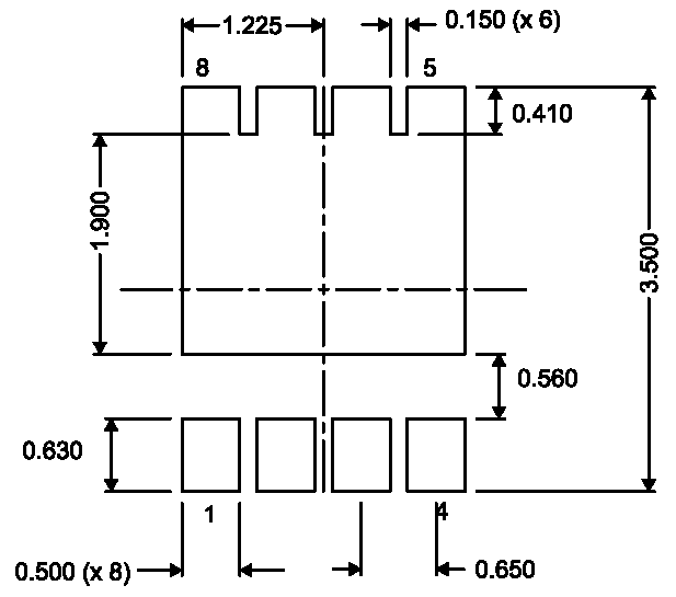
7.2 Recommended PCB Pattern

For recommended circuit layout for PCB designs, see application note SLPA005 – Reducing Ringing Through PCB Layout Techniques.