SLPS447F July 2013 – February 2022 CSD17483F4
PRODUCTION DATA
- 1Features
- 2Applications
- 3Description
- 4Revision History
- 5Specifications
- 6Device and Documentation Support
- 7Mechanical, Packaging, and Orderable Information
Package Options
Refer to the PDF data sheet for device specific package drawings
Mechanical Data (Package|Pins)
- YJC|3
Thermal pad, mechanical data (Package|Pins)
Orderable Information
5.3 Typical MOSFET Characteristics
TA = 25°C (unless otherwise stated)
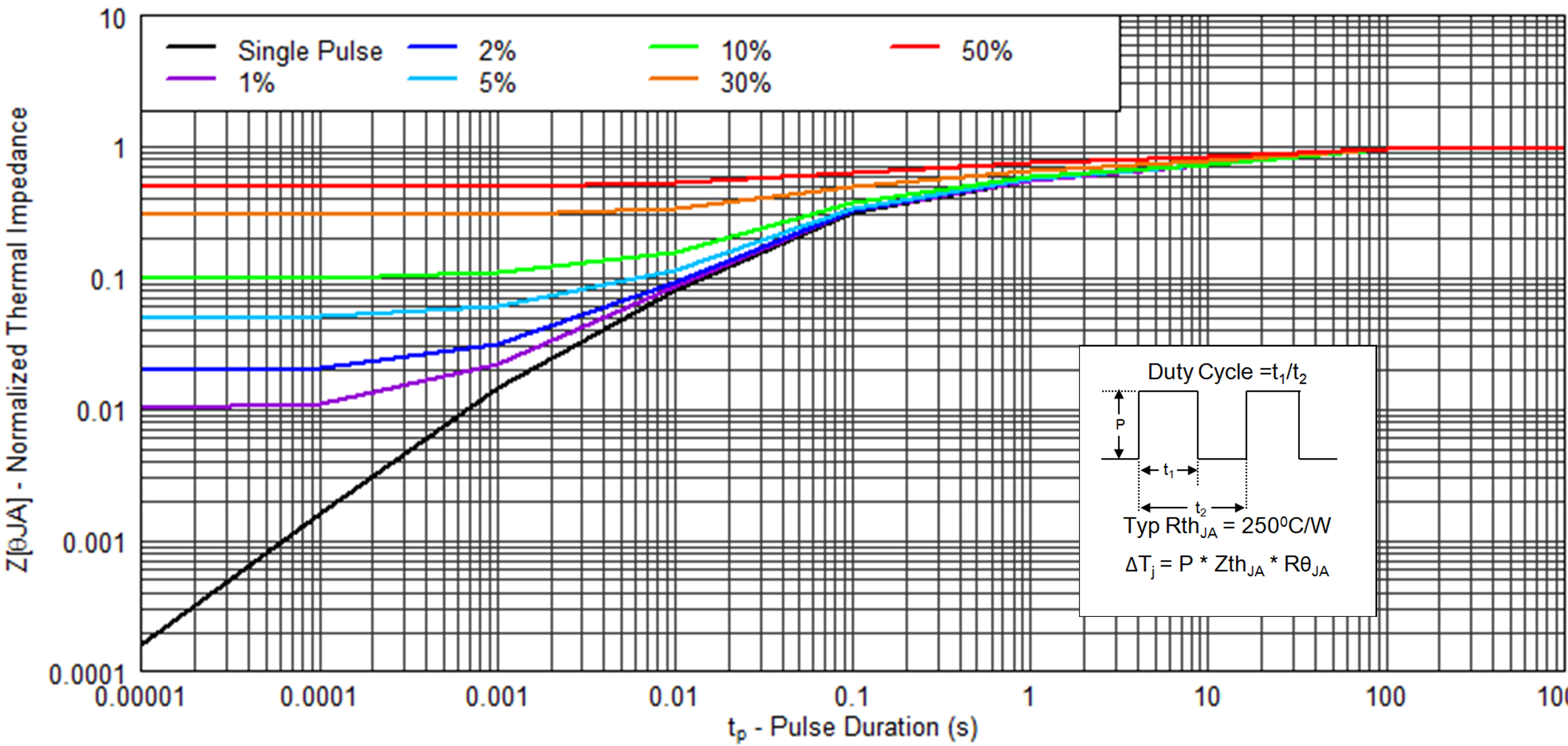 Figure 5-1 Transient
Thermal Impedance
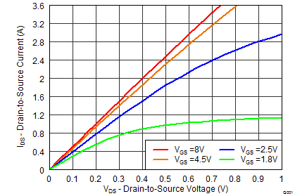 Figure 5-2 Saturation Characteristics
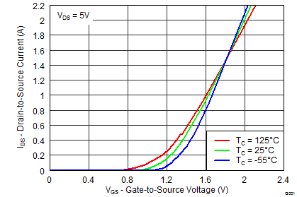 Figure 5-3 Transfer Characteristics
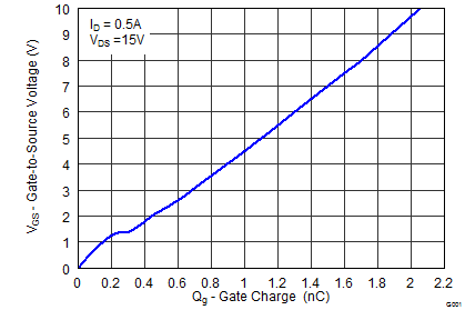 Figure 5-4 Gate Charge
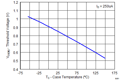 Figure 5-6 Threshold Voltage vs Temperature
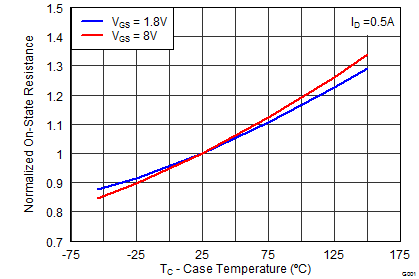 Figure 5-8 Normalized On-State Resistance vs Temperature
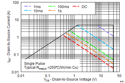 Figure 5-10 Maximum Safe Operating Area
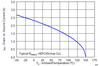 Figure 5-12 Maximum Drain Current vs Temperature
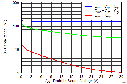 Figure 5-5 Capacitance
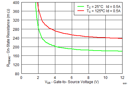 Figure 5-7 On-State Resistance vs Gate-to-Source Voltage
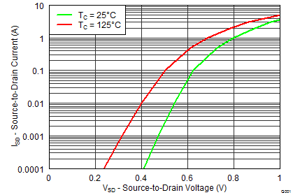 Figure 5-9 Typical Diode Forward Voltage
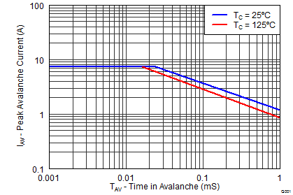 Figure 5-11 Single Pulse Unclamped Inductive Switching