-
CSD18511KTT 40-V N-Channel NexFET Power MOSFET
Package Options
Mechanical Data (Package|Pins)
- KTT|2
Thermal pad, mechanical data (Package|Pins)
Orderable Information
CSD18511KTT 40-V N-Channel NexFET Power MOSFET
1 Features
- Low Qg and Qgd
- Low RDS(ON)
- Low-Thermal Resistance
- Avalanche Rated
- Lead-Free Terminal Plating
- RoHS Compliant
- Halogen Free
- D2PAK Plastic Package
2 Applications
- Secondary Side Synchronous Rectifier
- Motor Control
3 Description
This 40-V, 2.1-mΩ, D2PAK (TO-263) NexFET™ power MOSFET is designed to minimize losses in power conversion applications.
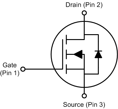
Product Summary
| TA = 25°C | TYPICAL VALUE | UNIT | ||
|---|---|---|---|---|
| VDS | Drain-to-Source Voltage | 40 | V | |
| Qg | Gate Charge Total (10 V) | 63.9 | nC | |
| Qgd | Gate Charge Gate-to-Drain | 9.7 | nC | |
| RDS(on) | Drain-to-Source On-Resistance | VGS = 4.5 V | 3.2 | mΩ |
| VGS = 10 V | 2.1 | |||
| VGS(th) | Threshold Voltage | 1.8 | V | |
Device Information(1)
| DEVICE | QTY | MEDIA | PACKAGE | SHIP |
|---|---|---|---|---|
| CSD18511KTT | 500 | 13-Inch Reel | D2PAK Plastic Package |
Tape and Reel |
| CSD18511KTTT | 50 |
- For all available packages, see the orderable addendum at the end of the data sheet.
Absolute Maximum Ratings
| TA = 25°C | VALUE | UNIT | |
|---|---|---|---|
| VDS | Drain-to-Source Voltage | 40 | V |
| VGS | Gate-to-Source Voltage | ±20 | V |
| ID | Continuous Drain Current (Package Limited) | 110 | A |
| Continuous Drain Current (Silicon Limited), TC = 25°C | 194 | ||
| Continuous Drain Current (Silicon Limited), TC = 100°C | 137 | ||
| IDM | Pulsed Drain Current(1) | 400 | A |
| PD | Power Dissipation | 188 | W |
| TJ, Tstg |
Operating Junction, Storage Temperature |
–55 to 175 | °C |
| EAS | Avalanche Energy, Single Pulse ID = 56 A, L = 0.1 mH, RG = 25 Ω |
156 | mJ |
- Max RθJC = 0.8°C/W, pulse duration ≤ 100 μs, duty cycle ≤ 1%.
RDS(on) vs VGS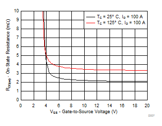 |
Gate Charge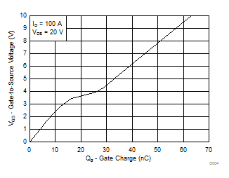 |
4 Revision History
| DATE | REVISION | NOTES |
|---|---|---|
| July 2017 | * | Initial release. |
5 Specifications
5.1 Electrical Characteristics
TA = 25°C (unless otherwise stated)| PARAMETER | TEST CONDITIONS | MIN | TYP | MAX | UNIT | ||
|---|---|---|---|---|---|---|---|
| STATIC CHARACTERISTICS | |||||||
| BVDSS | Drain-to-source voltage | VGS = 0 V, ID = 250 μA | 40 | V | |||
| IDSS | Drain-to-source leakage current | VGS = 0 V, VDS = 32 V | 1 | μA | |||
| IGSS | Gate-to-source leakage current | VDS = 0 V, VGS = 20 V | 100 | nA | |||
| VGS(th) | Gate-to-source threshold voltage | VDS = VGS, ID = 250 μA | 1.5 | 1.8 | 2.4 | V | |
| RDS(on) | Drain-to-source on-resistance | VGS = 4.5 V, ID = 100 A | 3.2 | 4.2 | mΩ | ||
| VGS = 10 V, ID = 100 A | 2.1 | 2.6 | |||||
| gfs | Transconductance | VDS = 4 V, ID = 100 A | 249 | S | |||
| DYNAMIC CHARACTERISTICS | |||||||
| Ciss | Input capacitance | VGS = 0 V, VDS = 20 V, ƒ = 1 MHz | 4570 | 5940 | pF | ||
| Coss | Output capacitance | 454 | 591 | pF | |||
| Crss | Reverse transfer capacitance | 235 | 306 | pF | |||
| RG | Series gate resistance | 0.9 | 1.8 | Ω | |||
| Qg | Gate charge total (4.5 V) | VDS = 20 V, ID = 100 A | 31 | nC | |||
| Qg | Gate charge total (10 V) | 64 | nC | ||||
| Qgd | Gate charge gate-to-drain | 9.7 | nC | ||||
| Qgs | Gate charge gate-to-source | 17.9 | nC | ||||
| Qg(th) | Gate charge at Vth | 7.4 | nC | ||||
| Qoss | Output charge | VDS = 20 V, VGS = 0 V | 20.7 | nC | |||
| td(on) | Turnon delay time | VDS = 20 V, VGS = 10 V, IDS = 100 A, RG = 0 Ω |
8 | ns | |||
| tr | Rise time | 6 | ns | ||||
| td(off) | Turnoff delay time | 17 | ns | ||||
| tf | Fall time | 3 | ns | ||||
| DIODE CHARACTERISTICS | |||||||
| VSD | Diode forward voltage | ISD = 100 A, VGS = 0 V | 0.9 | 1.0 | V | ||
| Qrr | Reverse recovery charge | VDS= 20 V, IF = 100 A, di/dt = 300 A/μs |
62 | nC | |||
| trr | Reverse recovery time | 31 | ns | ||||
5.2 Thermal Information
TA = 25°C (unless otherwise stated)| THERMAL METRIC | MIN | TYP | MAX | UNIT | |
|---|---|---|---|---|---|
| RθJC | Junction-to-case thermal resistance | 0.8 | °C/W | ||
| RθJA | Junction-to-ambient thermal resistance | 62 | °C/W | ||
5.3 Typical MOSFET Characteristics
TA = 25°C (unless otherwise stated)


| VDS = 5 V | ||

| VDS = 20 V | ID = 100 A | ||

| ID = 250 µA | ||

| ID = 100 A | ||

| Single pulse, max RθJC = 0.8°C/W | ||

| Max RθJC = 0.8°C/W | ||


6 Device and Documentation Support
6.1 Receiving Notification of Documentation Updates
To receive notification of documentation updates, navigate to the device product folder on ti.com. In the upper right corner, click on Alert me to register and receive a weekly digest of any product information that has changed. For change details, review the revision history included in any revised document.
6.2 Community Resources
The following links connect to TI community resources. Linked contents are provided "AS IS" by the respective contributors. They do not constitute TI specifications and do not necessarily reflect TI's views; see TI's Terms of Use.
-
TI E2E™ Online Community TI's Engineer-to-Engineer (E2E) Community. Created to foster collaboration among engineers. At e2e.ti.com, you can ask questions, share knowledge, explore ideas and help solve problems with fellow engineers.
-
Design Support TI's Design Support Quickly find helpful E2E forums along with design support tools and contact information for technical support.
6.3 Trademarks
NexFET, E2E are trademarks of Texas Instruments.
PowerPAD is a trademark of TI.
6.4 Electrostatic Discharge Caution

These devices have limited built-in ESD protection. The leads should be shorted together or the device placed in conductive foam during storage or handling to prevent electrostatic damage to the MOS gates.
6.5 Glossary
SLYZ022 — TI Glossary.
This glossary lists and explains terms, acronyms, and definitions.
7 Mechanical, Packaging, and Orderable Information
The following pages include mechanical, packaging, and orderable information. This information is the most current data available for the designated devices. This data is subject to change without notice and revision of this document. For browser-based versions of this data sheet, refer to the left-hand navigation.
7.1 KTT Package Dimensions

Notes:
- All linear dimensions are in millimeters. Any dimensions in parenthesis are for reference only. Dimensioning and tolerancing per ASME Y14.5M.
- This drawing is subject to change without notice.
- Features may not exist and shape may vary per different assembly sites.
Table 1. Pin Configuration
| POSITION | DESIGNATION |
|---|---|
| Pin 1 | Gate |
| Pin 2 / Tab | Drain |
| Pin 3 | Source |
7.2 Recommended PCB Pattern
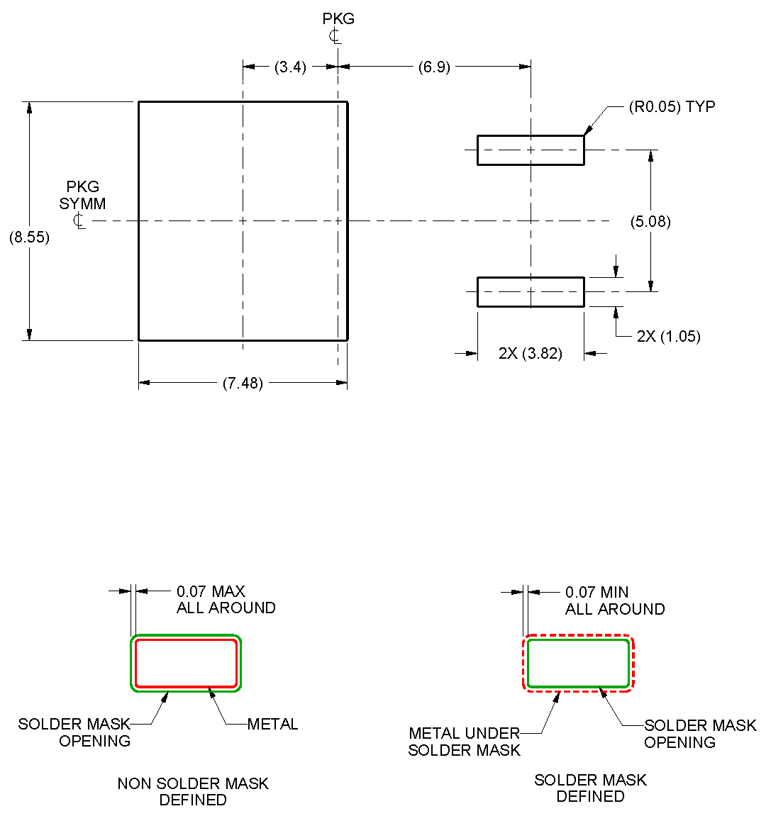
For recommended circuit layout for PCB designs, see Reducing Ringing Through PCB Layout Techniques (SLPA005).
7.3 Recommended Stencil Opening (0.125 mm Stencil Thickness)

Notes:
- This package is designed to be soldered to a thermal pad on the board. See PowerPAD™ Thermally Enhanced Package (SLMA002) and PowerPAD™ Made Easy (SLMA004) for more information.
- Laser cutting apertures with trapezoidal walls and rounded corners may offer better paste release. IPC-7525 may have alternate design recommendations.
- Board assembly site may have different recommendations for stencil design.