SLPS361C August 2012 – March 2024 CSD18532KCS
PRODUCTION DATA
- 1
- 1Features
- 2Applications
- Description
- 3Specifications
- 4Device and Documentation Support
- 5Revision History
- 6Mechanical Data
Package Options
Refer to the PDF data sheet for device specific package drawings
Mechanical Data (Package|Pins)
- KCS|3
Thermal pad, mechanical data (Package|Pins)
Orderable Information
Abstract
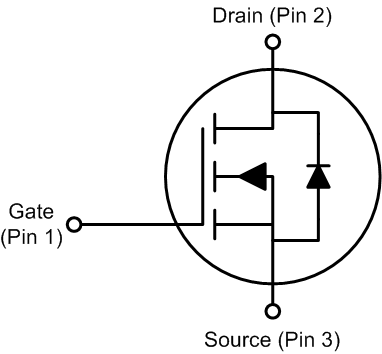
This 60V, 3.3mΩ, TO-220 NexFET™ power MOSFET is designed to minimize losses in power conversion applications.
 |
 |
Product Summary
| TA = 25°C | TYPICAL VALUE | UNIT | ||
|---|---|---|---|---|
| VDS | Drain-to-Source Voltage | 60 | V | |
| Qg | Gate Charge Total (10V) | 44 | nC | |
| Qgd | Gate Charge Gate-to-Drain | 6.9 | nC | |
| RDS(on) | Drain-to-Source On Resistance | VGS = 4.5V | 4.2 | mΩ |
| VGS = 10V | 3.3 | mΩ | ||
| VGS(th) | Threshold Voltage | 1.8 | V | |
Ordering Information(1)
| Device | Package | Media | Qty | Ship |
|---|---|---|---|---|
| CSD18532KCS | TO-220 Plastic Package | Tube | 50 | Tube |
(1) For all available packages, see the orderable addendum at the end of the data sheet.
Absolute Maximum Ratings
| TA = 25°C | VALUE | UNIT | |
|---|---|---|---|
| VDS | Drain-to-Source Voltage | 60 | V |
| VGS | Gate-to-Source Voltage | ±20 | V |
| ID | Continuous Drain Current (Package limited), TC = 25°C | 100 | A |
| Continuous Drain Current (Silicon limited), TC = 25°C | 169 | ||
| Continuous Drain Current (Silicon limited), TC = 100°C | 116 | ||
| IDM | Pulsed Drain Current (1) | 400 | A |
| PD | Power Dissipation | 250 | W |
| TJ, Tstg | Operating Junction and Storage Temperature Range | –55 to 175 | °C |
| EAS | Avalanche Energy, single
pulse ID = 75A, L = 0.1mH, RG = 25Ω | 281 | mJ |
(1) Pulse duration ≤300μs, duty cycle ≤2%
 vs VGS") RDS(on) vs VGS
RDS(on) vs VGS |
 Gate
Charge
Gate
Charge |