SLPS589 March   2016 CSD18535KTT

PRODUCTION DATA.  

  1. 1Features
  2. 2Applications
  3. 3Description
  4. 4Revision History
  5. 5Specifications
    1. 5.1 Electrical Characteristics
    2. 5.2 Thermal Information
    3. 5.3 Typical MOSFET Characteristics
  6. 6Device and Documentation Support
    1. 6.1 Community Resources
    2. 6.2 Trademarks
    3. 6.3 Electrostatic Discharge Caution
    4. 6.4 Glossary
  7. 7Mechanical, Packaging, and Orderable Information
    1. 7.1 KTT Package Dimensions
    2. 7.2 Recommended PCB Pattern
    3. 7.3 Recommended Stencil Opening (0.125 mm Stencil Thickness)

Package Options

Refer to the PDF data sheet for device specific package drawings

Mechanical Data (Package|Pins)
  • KTT|2
Thermal pad, mechanical data (Package|Pins)
Orderable Information

5 Specifications

5.1 Electrical Characteristics

(TA = 25°C unless otherwise stated)
PARAMETER TEST CONDITIONS MIN TYP MAX UNIT
STATIC CHARACTERISTICS
BVDSS Drain-to-source voltage VGS = 0 V, ID = 250 μA 60 V
IDSS Drain-to-source leakage current VGS = 0 V, VDS = 48 V 1 μA
IGSS Gate-to-source leakage current VDS = 0 V, VGS = 20 V 100 nA
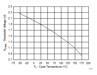
VGS(th) Gate-to-source threshold voltage VDS = VGS, ID = 250 μA 1.4 1.9 2.4 V
RDS(on) Drain-to-source on-resistance VGS = 4.5 V, ID = 100 A 2.3 2.9
VGS = 10 V, ID = 100 A 1.6 2.0
gfs Transconductance VDS = 6 V, ID = 100 A 263 S
DYNAMIC CHARACTERISTICS
Ciss Input capacitance VGS = 0 V, VDS = 30 V, ƒ = 1 MHz 5090 6620 pF
Coss Output capacitance 890 1150 pF
Crss Reverse transfer capacitance 24 31 pF
RG Series gate resistance 0.8 1.6 Ω
Qg Gate charge total (10 V) VDS = 30 V, ID = 100 A 63 81 nC
Qgd Gate charge gate-to-drain 10.4 nC
Qgs Gate charge gate-to-source 15.7 nC
Qg(th) Gate charge at Vth 9.4 nC
Qoss Output charge VDS = 30 V, VGS = 0 V 140 nC
td(on) Turn on delay time VDS = 30 V, VGS = 10 V,
IDS = 100 A, RG = 0 Ω
9 ns
tr Rise time 3 ns
td(off) Turn off delay time 19 ns
tf Fall time 3 ns
DIODE CHARACTERISTICS
VSD Diode forward voltage ISD = 100 A, VGS = 0 V 0.9 1.0 V
Qrr Reverse recovery charge VDS= 30 V, IF = 100 A,
di/dt = 300 A/μs
214 nC
trr Reverse recovery time 63 ns

5.2 Thermal Information

(TA = 25°C unless otherwise stated)
THERMAL METRIC MIN TYP MAX UNIT
RθJC Junction-to-case thermal resistance 0.5 °C/W
RθJA Junction-to-ambient thermal resistance 62 °C/W

5.3 Typical MOSFET Characteristics

(TA = 25°C unless otherwise stated)
CSD18535KTT D001_SLPS589.png
Figure 1. Transient Thermal Impedance
CSD18535KTT D002_SLPS589.gif
Figure 2. Saturation Characteristics
CSD18535KTT D003_SLPS589.gif
VDS = 5 V
Figure 3. Transfer Characteristics
CSD18535KTT D004_SLPS589.gif
VDS = 30 V ID = 100 A
Figure 4. Gate Charge
CSD18535KTT D006_SLPS589.gif
ID = 250 µA
Figure 6. Threshold Voltage vs Temperature
CSD18535KTT D008_SLPS589.gif
ID = 100 A
Figure 8. Normalized On-State Resistance vs Temperature
CSD18535KTT D010_SLPS589.gif
Single Pulse, Max RθJC = 0.5°C/W
Figure 10. Maximum Safe Operating Area
CSD18535KTT D012_SLPS589.gif
Figure 12. Maximum Drain Current vs Temperature
CSD18535KTT D005_SLPS589.gif
Figure 5. Capacitance
CSD18535KTT D007_SLPS589.gif
Figure 7. On-State Resistance vs Gate-to-Source Voltage
CSD18535KTT D009_SLPS589.gif
Figure 9. Typical Diode Forward Voltage
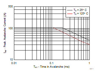
CSD18535KTT D011_SLPS589.gif
Figure 11. Single Pulse Unclamped Inductive Switching