SLPS539B March 2015 – January 2017 CSD19535KTT
PRODUCTION DATA.
- 1Features
- 2Applications
- 3Description
- 4Revision History
- 5Specifications
- 6Device and Documentation Support
- 7Mechanical, Packaging, and Orderable Information
Package Options
Refer to the PDF data sheet for device specific package drawings
Mechanical Data (Package|Pins)
- KTT|2
Thermal pad, mechanical data (Package|Pins)
Orderable Information
7 Mechanical, Packaging, and Orderable Information
The following pages include mechanical, packaging, and orderable information. This information is the most current data available for the designated devices. This data is subject to change without notice and revision of this document. For browser-based versions of this data sheet, refer to the left-hand navigation.
7.1 KTT Package Dimensions

Notes:
- All linear dimensions are in millimeters. Any dimensions in parenthesis are for reference only. Dimensioning and tolerancing per ASME Y14.5M.
- This drawing is subject to change without notice.
- Features may not exist and shape may vary per different assembly sites.
Table 1. Pin Configuration
| POSITION | DESIGNATION |
|---|---|
| Pin 1 | Gate |
| Pin 2 / Tab | Drain |
| Pin 3 | Source |
7.2 Recommended PCB Pattern

For recommended circuit layout for PCB designs, see Reducing Ringing Through PCB Layout Techniques (SLPA005).
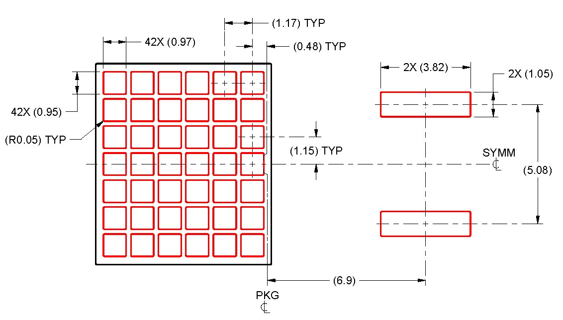
7.3 Recommended Stencil Opening (0.125 mm Stencil Thickness)

Notes:
- This package is designed to be soldered to a thermal pad on the board. See application notes PowerPAD™ Thermally Enhanced Package (SLMA002) and PowerPAD™ Made Easy (SLMA004) for more information.
- Laser cutting apertures with trapezoidal walls and rounded corners may offer better paste release. IPC-7525 may have alternate design recommendations.
- Board assembly site may have different recommendations for stencil design.