SLPS431B June   2013  – December  2014 CSD22202W15

PRODUCTION DATA.  

  1. 1Features
  2. 2Applications
  3. 3Description
  4. 4Revision History
  5. 5Specifications
    1. 5.1 Electrical Characteristics
    2. 5.2 Thermal Information
    3. 5.3 Typical MOSFET Characteristics
  6. 6Device and Documentation Support
    1. 6.1 Trademarks
    2. 6.2 Electrostatic Discharge Caution
    3. 6.3 Glossary
  7. 7Mechanical, Packaging, and Orderable Information
    1. 7.1 CSD22202W15 Package Dimensions
    2. 7.2 Recommended Land Pattern
    3. 7.3 Tape and Reel Information

Package Options

Refer to the PDF data sheet for device specific package drawings

Mechanical Data (Package|Pins)
  • YZF|9
Thermal pad, mechanical data (Package|Pins)
Orderable Information

5 Specifications

5.1 Electrical Characteristics

(TA = 25°C unless otherwise stated)
PARAMETER TEST CONDITIONS MIN TYP MAX UNIT
STATIC CHARACTERISTICS
BVDSS Drain-to-Source Voltage VGS = 0 V, IDS = –250 μA –8 V
BVGSS Gate-to-Source Voltage VDS = 0 V, IG = –250 μA –6 V
IDDS Drain-to-Source Leakage Current VGS = 0 V, VDS = –6.4 V –1 μA
IGSS Gate-to-Source Leakage Current VDS = 0 V, VGS = –6 V –100 nA
VGS(th) Gate-to-Source Threshold Voltage VDS = VGS, IDS = –250 μA –0.6 –0.8 –1.1 V
RDS(on) Drain-to-Source On-Resistance VGS = –2.5 V, IDS = –2 A 14.5 17.4
VGS = –4.5 V, IDS = –2 A 10.2 12.2
gƒs Transconductance VDS = –4 V, IDS = –2 A 15.3 S
DYNAMIC CHARACTERISTICS
CISS Input Capacitance VGS = 0 V, VDS = –4 V,
ƒ = 1 MHz
1060 1390 pF
COSS Output Capacitance 588 765 pF
CRSS Reverse Transfer Capacitance 192 250 pF
RG Series Gate Resistance 28 Ω
Qg Gate Charge Total (–4.5 V) VDS = –4 V,
ID = –2 A
6.5 8.4 nC
Qgd Gate Charge - Gate-to-Drain 1 nC
Qgs Gate Charge - Gate-to-Source 1.6 nC
Qg(th) Gate Charge at Vth 0.8 nC
QOSS Output Charge VDS = –4 V, VGS = 0 V 2.7 nC
td(on) Turn On Delay Time VDS = –4 V, VGS = –4.5 V,
IDS = –2 A, RG = 10 Ω
10.4 ns
tr Rise Time 8.4 ns
td(off) Turn Off Delay Time 109 ns
tƒ Fall Time 38 ns
DIODE CHARACTERISTICS
VSD Diode Forward Voltage IDS = –2 A, VGS = 0 V –0.75 –1 V
Qrr Reverse Recovery Charge VDS = –4 V, IF = –2 A,
di/dt = 200 A/μs
22 nC
trr Reverse Recovery Time 19 ns

5.2 Thermal Information

(TA = 25°C unless otherwise stated)
THERMAL METRIC TYPICAL VALUES UNIT
RθJA Junction-to-Ambient Thermal Resistance(1) 75 °C/W
Junction-to-Ambient Thermal Resistance(2) 210
(1) Device mounted on FR4 material with 1-inch2 (6.45-cm2), 2-oz. (0.071-mm thick) Cu.
(2) Device mounted on FR4 material with minimum Cu mounting area.
M0149-01_LPS266.gif
Typ RθJA = 75°C/W when mounted on 1inch2 of 2 oz. Cu.
M0150-01_LPS266.gif
Typ RθJA = 210°C/W when mounted on minimum pad area of
2 oz. Cu.

5.3 Typical MOSFET Characteristics

(TA = 25°C unless otherwise stated)
graph01p2_LPS400.png
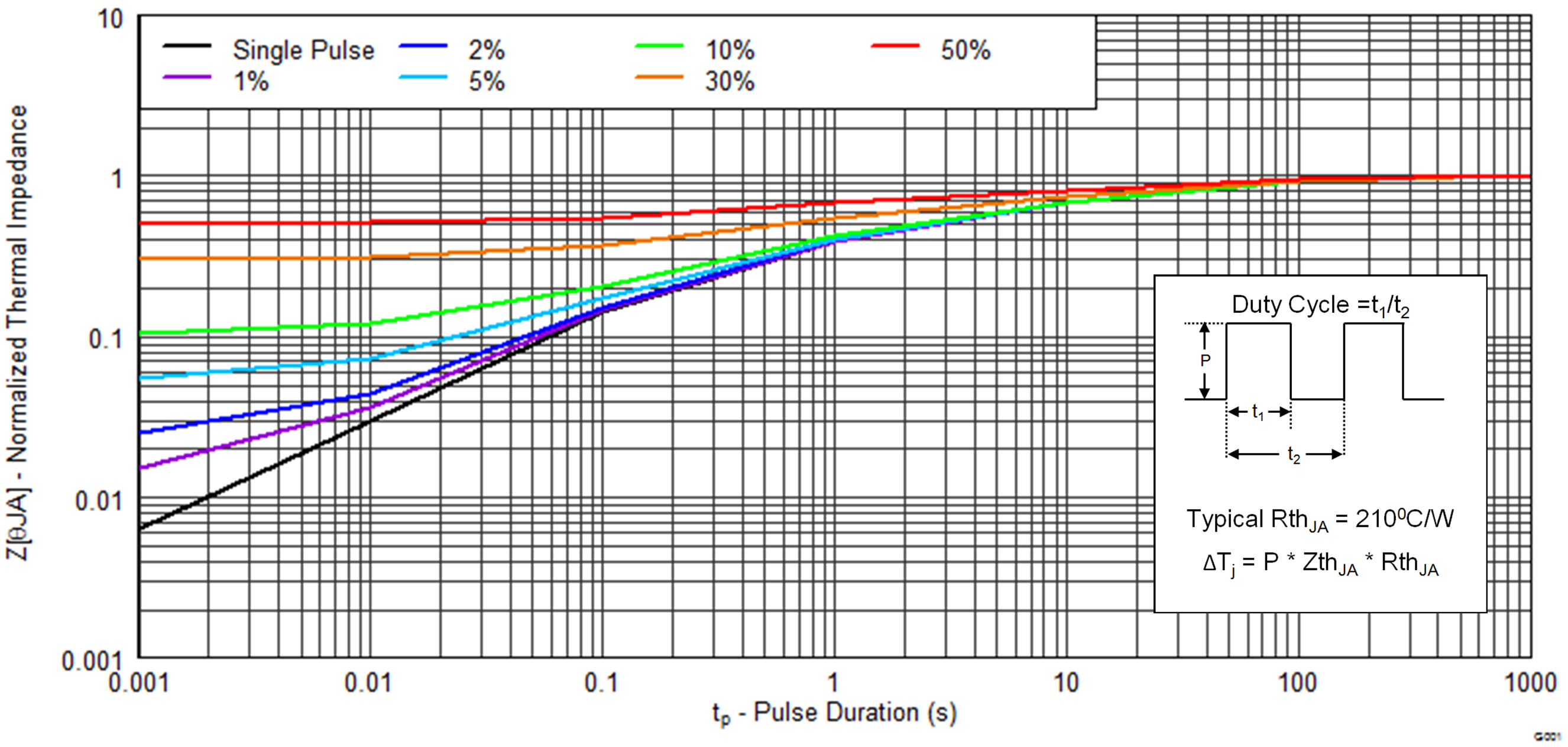
Figure 1. Transient Thermal Impedance
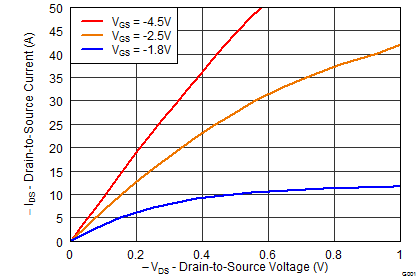
graph02_LPS400.png
Figure 2. Saturation Characteristics
graph04_LPS400.png
Figure 4. Gate Charge
graph06_LPS400.png
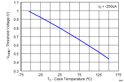
Figure 6. Threshold Voltage vs Temperature
graph08p2_LPS400.png
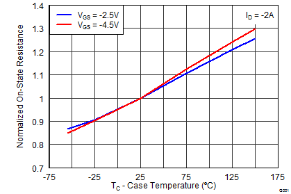
Figure 8. Normalized On-State Resistance vs Temperature
graph10p2_LPS400.png
Figure 10. Maximum Safe Operating Area
graph12p2_LPS400.png
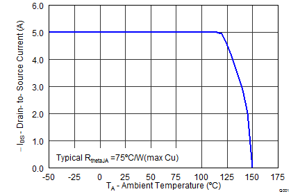
Figure 12. Maximum Drain Current vs Temperature
graph03_LPS400.png
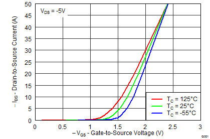
Figure 3. Transfer Characteristics
graph05_LPS400.png
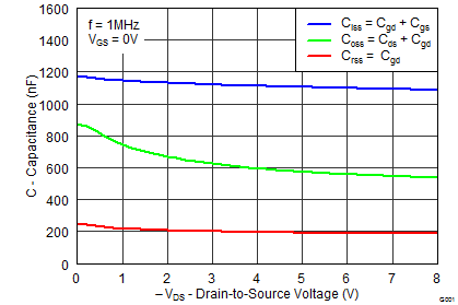
Figure 5. Capacitance
graph07p2_LPS400.png
Figure 7. On-State Resistance vs Gate-to-Source Voltage
graph09p2_LPS400.png
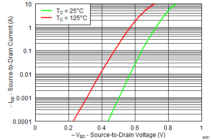
Figure 9. Typical Diode Forward Voltage
graph11_LPS400.png
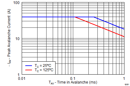
Figure 11. Single Pulse Unclamped Inductive Switching