CSD25202W15 20-V P-Channel NexFET Power MOSFET
1 Features
- Low-Resistance
- Small Footprint 1.5 mm × 1.5 mm
- Gate ESD Protection –3 kV
- Pb Free
- RoHS Compliant
- Halogen Free
- Gate-Source Voltage Clamp
2 Applications
- Battery Management
- Battery Protection
3 Description
This 21 mΩ, 20 V device is designed to deliver the lowest on resistance and gate charge in a small 1.5 mm × 1.5 mm chip scale package with excellent thermal characteristics in an ultra-low profile. Low on resistance coupled with the small footprint and low profile make the device ideal for battery operated space constrained applications.

Product Summary
Ordering Information(1)
| Device | Qty | Media | Package | Ship |
|---|---|---|---|---|
| CSD25202W15 | 3000 | 7-Inch Reel | 1.5-mm × 1.5-mm Wafer Level Package | Tape and Reel |
| CSD25202W15T | 250 | 7-Inch Reel |
- For all available packages, see the orderable addendum at the end of the data sheet.
Absolute Maximum Ratings
| TA = 25°C | VALUE | UNIT | |
|---|---|---|---|
| VDS | Drain-to-Source Voltage | –20 | V |
| VGS | Gate-to-Source Voltage | –6 | V |
| ID | Continuous Drain Current(1) | –4 | A |
| Pulsed Drain Current(2) | –38 | A | |
| IG | Continuous Gate Current(1) | –0.5 | A |
| Pulsed Gate Current(2) | –7 | A | |
| PD | Power Dissipation | 0.5 | W |
| TJ, Tstg |
Operating Junction and Storage Temperature Range |
–55 to 150 | °C |
- Ball limited
- Typical RθJA = 220ºC/W, pulse duration ≤100 µs, duty cycle ≤ 1%
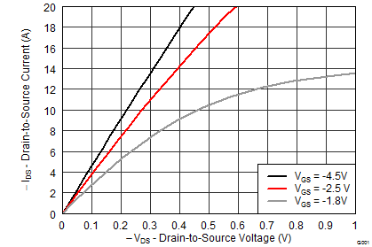
RDS(on) vs VGS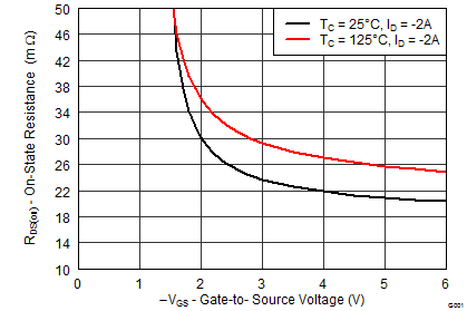 |
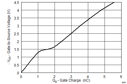
Gate Charge |
4 Revision History
Changes from * Revision (June 2014) to A Revision
- Corrected "Drain-to-Drain Voltage" to state "Drain-to-Source Voltage"Go
5 Specifications
5.1 Electrical Characteristics
(TA = 25°C unless otherwise stated)| PARAMETER | TEST CONDITIONS | MIN | TYP | MAX | UNIT | ||
|---|---|---|---|---|---|---|---|
| STATIC CHARACTERISTICS | |||||||
| BVDSS | Drain-to-Source Voltage | VGS = 0 V, IDS = –250 μA | –20 | V | |||
| BVGSS | Gate-to-Source Voltage | VDS = 0 V, IG = –250 μA | –6 | –7.2 | V | ||
| IDDS | Drain-to-Source Leakage Current | VGS = 0 V, VDS = –16 V | –1 | μA | |||
| IGSS | Gate-to-Source Leakage Current | VDS = 0 V, VGS = –6 V | –100 | nA | |||
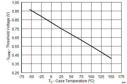
| VGS(th) | Gate-to-Source Threshold Voltage | VDS = VGS, IDS = –250 μA | –0.45 | –0.75 | –1.05 | V | |
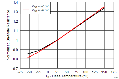
| RDS(on) | Drain-to-Source On Resistance | VGS = –1.8 V, IDS = –2 A | 40 | 52 | mΩ | ||
| VGS = –2.5 V, IDS = –2 A | 26 | 32 | mΩ | ||||
| VGS = –4.5 V, IDS = –2 A | 21 | 26 | mΩ | ||||
| gƒs | Transconductance | VDS = –2 V, IDS = –2 A | 16 | S | |||
| DYNAMIC CHARACTERISTICS | |||||||
| CISS | Input Capacitance | VGS = 0 V, VDS = –10 V, ƒ = 1 MHz |
778 | 1010 | pF | ||
| COSS | Output Capacitance | 400 | 520 | pF | |||
| CRSS | Reverse Transfer Capacitance | 21 | 27 | pF | |||
| RG | Series Gate Resistance(1) | 31 | Ω | ||||
| Qg | Gate Charge Total (–4.5 V) | VDS = –10 V, ID = –2 A |
5.8 | 7.5 | nC | ||
| Qgd | Gate Charge - Gate-to-Drain | 0.8 | nC | ||||
| Qgs | Gate Charge - Gate-to-Source | 1.1 | nC | ||||
| Qg(th) | Gate Charge at Vth | 0.6 | nC | ||||
| QOSS | Output Charge | VDS = –9.5 V, VGS = 0 V | 8.7 | nC | |||
| td(on) | Turn On Delay Time(2) | VDS = –10 V, VGS = –4.5 V, IDS = –2 A, RG = 2 Ω |
15 | ns | |||
| tr | Rise Time(2) | 12 | ns | ||||
| td(off) | Turn Off Delay Time(2) | 64 | ns | ||||
| tf | Fall Time(2) | 28 | ns | ||||
| DIODE CHARACTERISTICS | |||||||
| VSD | Diode Forward Voltage | IDS = –2 A, VGS = 0 V | –0.75 | –1 | V | ||
| Qrr | Reverse Recovery Charge | VSD = –10 V, IF = –2 A, di/dt = 200 A/μs |
19 | nC | |||
| trr | Reverse Recovery Time | 26 | ns | ||||
5.2 Thermal Information
(TA = 25°C unless otherwise stated)| THERMAL METRIC | MIN | TYP | MAX | UNIT | |
|---|---|---|---|---|---|
| RθJA | Junction-to-Ambient Thermal Resistance(1) | 220 | °C/W | ||
| Junction-to-Ambient Thermal Resistance(2) | 140 | ||||
 |
Typ RθJA = 140°C/W when mounted on 1 inch2 (6.45 cm2) of 2-oz. (0.071-mm thick) Cu. |
 |
Typ RθJA = 220°C/W when mounted on a minimum pad area of 2-oz. (0.071-mm thick) Cu. |
5.3 Typical MOSFET Characteristics
(TA = 25°C unless otherwise stated)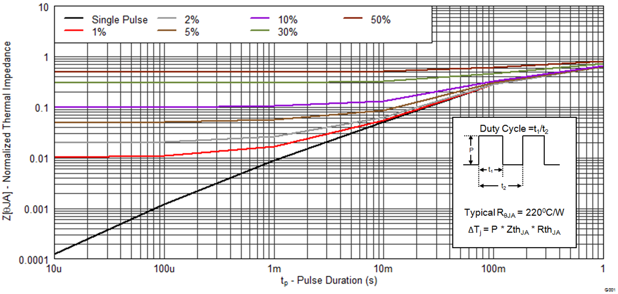
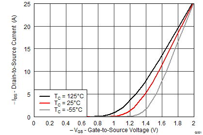
| ID = –2 A | VDS = –10 V | |
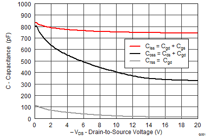
| ID = –250 µA | ||
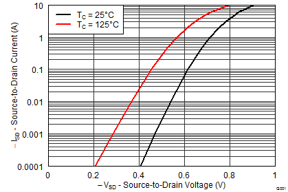
| ID = –2 A | ||
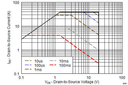
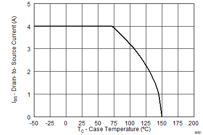
| Single Pulse, Max RθJA = 220°C/W | ||
| VDS = –5 V | ||
6 Device and Documentation Support
6.1 Trademarks
All other trademarks are the property of their respective owners.
6.2 Electrostatic Discharge Caution

These devices have limited built-in ESD protection. The leads should be shorted together or the device placed in conductive foam during storage or handling to prevent electrostatic damage to the MOS gates.
6.3 Glossary
SLYZ022 — TI Glossary.
This glossary lists and explains terms, acronyms, and definitions.