SLPS692C October 2017 – June 2024 CSD25501F3
PRODUCTION DATA
- 1
- 1Features
- 2Applications
- 3Description
- 4Specifications
- 5Device and Documentation Support
- 6Revision History
- 7Mechanical, Packaging, and Orderable Information
Package Options
Refer to the PDF data sheet for device specific package drawings
Mechanical Data (Package|Pins)
- YJN|3
Thermal pad, mechanical data (Package|Pins)
Orderable Information
3 Description
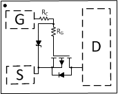
This –20V, 64mΩ, P-Channel FemtoFET™ MOSFET is designed and optimized to minimize the footprint in many handheld and mobile applications. This technology is capable of replacing standard small signal MOSFETs while providing a substantial reduction in footprint size. The integrated 10kΩ clamp resistor (RC) allows the gate voltage (VGS) to be operated above the maximum internal gate oxide value of –6V, depending on duty cycle. The gate leakage (IGSS) through the diode increases as VGS is increased above –6V.
| TA = 25°C | TYPICAL VALUE | UNIT | ||
|---|---|---|---|---|
| VDS | Drain-to-Source Voltage | –20 | V | |
| Qg | Gate Charge Total (–4.5V) | 1.02 | nC | |
| Qgd | Gate Charge Gate-to-Drain | 0.09 | nC | |
| RDS(on) | Drain-to-Source On-Resistance |
VGS = –1.8V | 120 | mΩ |
| VGS = –2.5V | 86 | |||
| VGS = –4.5V | 64 | |||
| VGS(th) | Threshold Voltage | –0.75 | V | |
| DEVICE(1) | QTY | MEDIA | PACKAGE | SHIP |
|---|---|---|---|---|
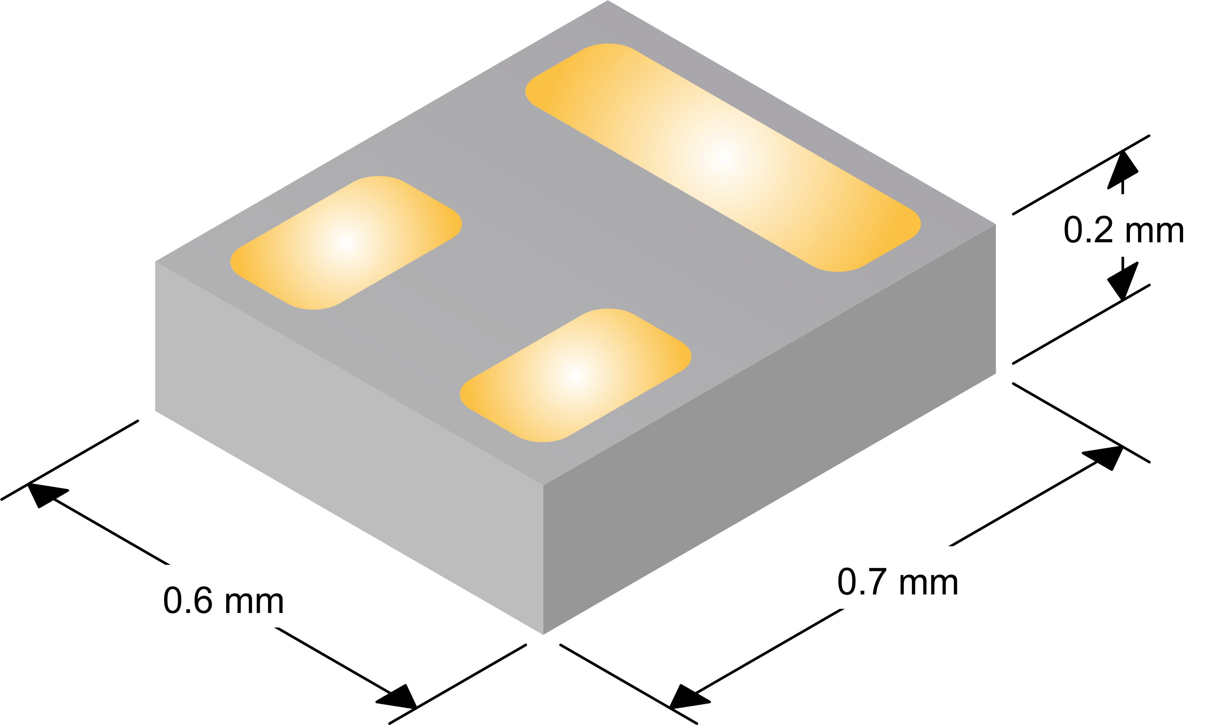
| CSD25501F3 | 3000 | 7 Inch Reel | Femto 0.73mm × 0.64mm Land Grid Array (LGA) |
Tape and Reel |
| CSD25501F3T | 250 |
| TA = 25°C (unless otherwise stated) | VALUE | UNIT | |
|---|---|---|---|
| VDS | Drain-to-Source Voltage | –20 | V |
| VGS | Gate-to-Source Voltage | –20 | V |
| ID | Continuous Drain Current(1) | –3.6 | A |
| IDM | Pulsed Drain Current(1)(2) | –13.6 | A |
| PD | Power Dissipation(1) | 500 | mW |
| V(ESD) | Human Body Model (HBM) | 4000 | V |
| Charged Device Model (CDM) | 2000 | ||
| TJ, Tstg |
Operating Junction, Storage Temperature |
–55 to 150 | °C |
 Typical Part Dimensions
 Top View