SLPS327B
September 2012 – April 2018
CSD86360Q5D
PRODUCTION DATA.
1
Features
2
Applications
3
Description
3.1
Top View
Device Images
4
Revision History
5
Specifications
5.1
Absolute Maximum Ratings
5.2
Recommended Operating Conditions
5.3
Power Block Performance
5.4
Thermal Information
5.5
Electrical Characteristics
5.6
Typical Power Block Device Characteristics
5.7
Typical Power Block MOSFET Characteristics
6
Application and Implementation
6.1
Application Information
6.1.1
Equivalent System Performance
6.1.2
Power Loss Curves
6.1.3
Safe Operating Area (SOA) Curves
6.1.4
Normalized Curves
6.2
Typical Application
6.2.1
Design Example: Calculating Power Loss and SOA
6.2.1.1
Operating Conditions
6.2.1.2
Calculating Power Loss
6.2.1.3
Calculating SOA Adjustments
7
Layout
7.1
Layout Guidelines
7.1.1
Electrical Performance
7.1.2
Thermal Performance
7.2
Layout Example
8
Device and Documentation Support
8.1
Documentation Support
8.1.1
Related Documentation
8.2
Receiving Notification of Documentation Updates
8.3
Community Resources
8.4
Trademarks
8.5
Electrostatic Discharge Caution
8.6
Glossary
9
Mechanical, Packaging, and Orderable Information
9.1
Q5D Package Dimensions
9.2
Land Pattern Recommendation
9.3
Stencil Recommendation
9.4
Q5D Tape and Reel Information
Package Options
Mechanical Data (Package|Pins)
DQY|8
MPSS031A
Thermal pad, mechanical data (Package|Pins)
Orderable Information
slps327b_oa
slps327b_pm
9.2
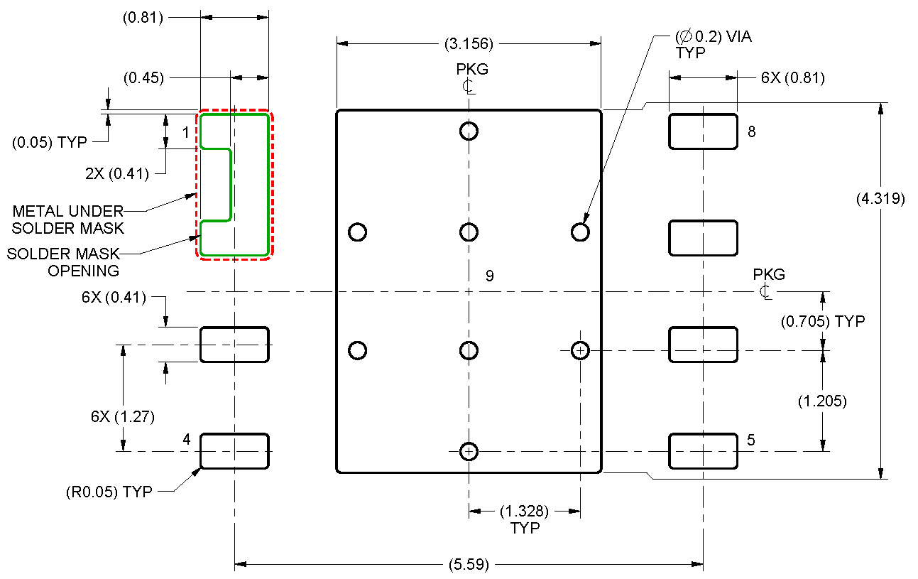
Land Pattern Recommendation
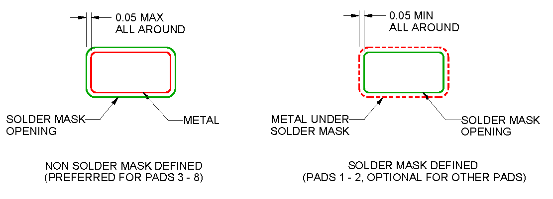
This package is designed to be soldered to a thermal pad on the board. For more information, see
QFN/SON PCB Attachment
(SLUA271).
Vias are optional depending on application, refer to device data sheet. If some or all are implemented, recommended via locations are shown.