SLPS327B September   2012  – April 2018 CSD86360Q5D

PRODUCTION DATA.  

  1. 1Features
  2. 2Applications
  3. 3Description
    1. 3.1 Top View
      1.      Device Images
  4. 4Revision History
  5. 5Specifications
    1. 5.1 Absolute Maximum Ratings
    2. 5.2 Recommended Operating Conditions
    3. 5.3 Power Block Performance
    4. 5.4 Thermal Information
    5. 5.5 Electrical Characteristics
    6. 5.6 Typical Power Block Device Characteristics
    7. 5.7 Typical Power Block MOSFET Characteristics
  6. 6Application and Implementation
    1. 6.1 Application Information
      1. 6.1.1 Equivalent System Performance
      2. 6.1.2 Power Loss Curves
      3. 6.1.3 Safe Operating Area (SOA) Curves
      4. 6.1.4 Normalized Curves
    2. 6.2 Typical Application
      1. 6.2.1 Design Example: Calculating Power Loss and SOA
        1. 6.2.1.1 Operating Conditions
        2. 6.2.1.2 Calculating Power Loss
        3. 6.2.1.3 Calculating SOA Adjustments
  7. 7Layout
    1. 7.1 Layout Guidelines
      1. 7.1.1 Electrical Performance
      2. 7.1.2 Thermal Performance
    2. 7.2 Layout Example
  8. 8Device and Documentation Support
    1. 8.1 Documentation Support
      1. 8.1.1 Related Documentation
    2. 8.2 Receiving Notification of Documentation Updates
    3. 8.3 Community Resources
    4. 8.4 Trademarks
    5. 8.5 Electrostatic Discharge Caution
    6. 8.6 Glossary
  9. 9Mechanical, Packaging, and Orderable Information
    1. 9.1 Q5D Package Dimensions
    2. 9.2 Land Pattern Recommendation
    3. 9.3 Stencil Recommendation
    4. 9.4 Q5D Tape and Reel Information

Package Options

Mechanical Data (Package|Pins)
Thermal pad, mechanical data (Package|Pins)
Orderable Information

Typical Power Block MOSFET Characteristics

TA = 25°C, unless stated otherwise.
CSD86360Q5D graph10_SLPS327.png
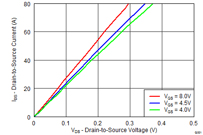
Figure 10. Control MOSFET Saturation
CSD86360Q5D graph12_SLPS287.png
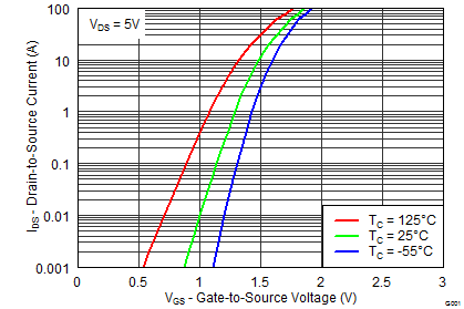
Figure 12. Control MOSFET Transfer
CSD86360Q5D graph14_SLPS327.png
Figure 14. Control MOSFET Gate Charge
CSD86360Q5D graph16_SLPS327.png
Figure 16. Control MOSFET Capacitance
CSD86360Q5D graph18_SLPS327.png
Figure 18. Control MOSFET VGS(th)
CSD86360Q5D graph20p2_SLPS327.png
Figure 20. Control MOSFET RDS(on) vs VGS
CSD86360Q5D graph22_SLPS327.png
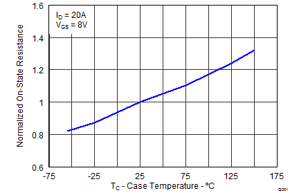
Figure 22. Control MOSFET Normalized RDS(on)
CSD86360Q5D graph24_SLPS327.png
Figure 24. Control MOSFET Body Diode
CSD86360Q5D graph26_SLPS327.png
Figure 26. Control MOSFET Unclamped Inductive Switching
CSD86360Q5D graph11_SLPS327.png
Figure 11. Sync MOSFET Saturation
CSD86360Q5D graph13_SLPS287.png
Figure 13. Sync MOSFET Transfer
CSD86360Q5D graph15_SLPS327.png
Figure 15. Sync MOSFET Gate Charge
CSD86360Q5D graph17_SLPS327.png
Figure 17. Sync MOSFET Capacitance
CSD86360Q5D graph19_SLPS327.png
Figure 19. Sync MOSFET VGS(th)
CSD86360Q5D graph21p2_SLPS327.png
Figure 21. Sync MOSFET RDS(on) vs VGS
CSD86360Q5D graph23_SLPS327.png
Figure 23. Sync MOSFET Normalized RDS(on)
CSD86360Q5D graph25_SLPS327.png
Figure 25. Sync MOSFET Body Diode
CSD86360Q5D graph27_SLPS327.png
Figure 27. Sync MOSFET Unclamped Inductive Switching