SLPS574B
February 2016 – April 2018
CSD87335Q3D
PRODUCTION DATA.
1
Features
2
Applications
3
Description
Top View
Device Images
4
Revision History
5
Specifications
5.1
Absolute Maximum Ratings
5.2
Recommended Operating Conditions
5.3
Thermal Information
5.4
Power Block Performance
5.5
Electrical Characteristics
5.6
Typical Power Block Device Characteristics
5.7
Typical Power Block MOSFET Characteristics
6
Applications and Implementation
6.1
Application Information
6.1.1
Equivalent System Performance
6.2
Power Loss Curves
6.3
Safe Operating Curves (SOA)
6.4
Normalized Curves
6.5
Calculating Power Loss and SOA
6.5.1
Design Example
6.5.2
Calculating Power Loss
6.5.3
Calculating SOA Adjustments
7
Recommended PCB Design Overview
7.1
Electrical Performance
7.2
Thermal Performance
8
Device and Documentation Support
8.1
Receiving Notification of Documentation Updates
8.2
Community Resources
8.3
Trademarks
8.4
Electrostatic Discharge Caution
8.5
Glossary
9
Mechanical, Packaging, and Orderable Information
9.1
Q3D Package Dimensions
9.2
Land Pattern Recommendation
9.3
Stencil Recommendation
9.4
Q3D Tape and Reel Information
9.5
Pin Configuration
Package Options
Mechanical Data (Package|Pins)
DQZ|8
MPSS032C
Thermal pad, mechanical data (Package|Pins)
Orderable Information
slps574b_oa
5.7
Typical Power Block MOSFET Characteristics
T
A
= 25°C, unless stated otherwise.
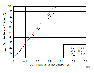
Figure 9.
Control MOSFET Saturation
V
DS
= 5 V
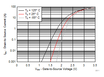
Figure 11.
Control MOSFET Transfer
I
D
= 15 A
V
DD
= 15 V
Figure 13.
Control MOSFET Gate Charge
Figure 15.
Control MOSFET Capacitance
I
D
= 250 µA
Figure 17.
Control MOSFET V
GS(th)
Figure 19.
Control MOSFET R
DS(on)
vs V
GS
I
D
= 15 A
V
GS
= 4.5 V
Figure 21.
Control MOSFET Normalized R
DS(on)
Figure 23.
Control MOSFET Body Diode
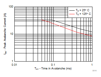
Figure 25.
Control MOSFET Unclamped Inductive Switching
Figure 10.
Sync MOSFET Saturation
V
DS
= 5 V
Figure 12.
Sync MOSFET Transfer
I
D
= 15 A
V
DD
= 15 V
Figure 14.
Sync MOSFET Gate Charge
Figure 16.
Sync MOSFET Capacitance
I
D
= 250 µA
Figure 18.
Sync MOSFET V
GS(th)
Figure 20.
Sync MOSFET R
DS(on)
vs V
GS
I
D
= 15 A
V
GS
= 4.5 V
Figure 22.
Sync MOSFET Normalized R
DS(on)
Figure 24.
Sync MOSFET Body Diode
Figure 26.
Sync MOSFET Unclamped Inductive Switching